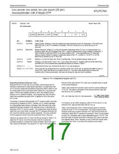
Philips Semiconductors
Preliminary data
Low power, low price, low pin count (20 pin)
microcontroller with 4 kbyte OTP
87LPC764
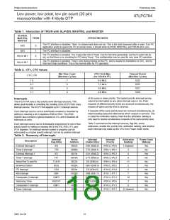
The value of port pins at reset is determined by the PRHI bit in the
UCFG1 register. Ports may be configured to reset high or low as
needed for the application. When port pins are driven high at reset,
they are in quasi-bidirectional mode and therefore do not source
large amounts of current.
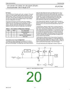
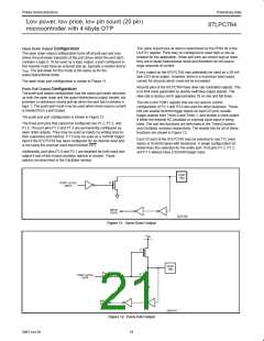
Open Drain Output Configuration
The open drain output configuration turns off all pull-ups and only
drives the pull-down transistor of the port driver when the port latch
contains a logic 0. To be used as a logic output, a port configured in
this manner must have an external pull-up, typically a resistor tied to
V
. The pull-down for this mode is the same as for the
DD
Every output on the 87LPC764 may potentially be used as a 20 mA
sink LED drive output. However, there is a maximum total output
current for all ports which must not be exceeded.
quasi-bidirectional mode.
The open drain port configuration is shown in Figure 11.
All ports pins of the 87LPC764 have slew rate controlled outputs. This
is to limit noise generated by quickly switching output signals. The
slew rate is factory set to approximately 10 ns rise and fall times.
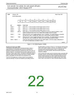
Push-Pull Output Configuration
The push-pull output configuration has the same pull-down structure
as both the open drain and the quasi-bidirectional output modes, but
provides a continuous strong pull-up when the port latch contains a
logic 1. The push-pull mode may be used when more source current
is needed from a port output.
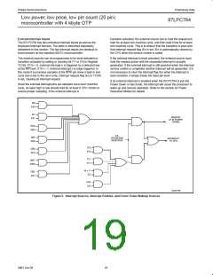
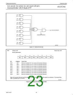
The bits in the P2M1 register that are not used to control
configuration of P2.1 and P2.0 are used for other purposes. These
bits can enable Schmitt trigger inputs on each I/O port, enable
toggle outputs from Timer 0 and Timer 1, and enable a clock output
if either the internal RC oscillator or external clock input is being
used. The last two functions are described in the Timer/Counters
and Oscillator sections respectively. The enable bits for all of these
functions are shown in Figure 13.
The push-pull port configuration is shown in Figure 12.
The three port pins that cannot be configured are P1.2, P1.3, and
P1.5. The port pins P1.2 and P1.3 are permanently configured as
open drain outputs. They may be used as inputs by writing ones to
their respective port latches. P1.5 may be used as a Schmitt trigger
input if the 87LPC764 has been configured for an internal reset and
is not using the external reset input function RST.
Each I/O port of the 87LPC764 may be selected to use TTL level
inputs or Schmitt inputs with hysteresis. A single configuration bit
determines this selection for the entire port. Port pins P1.2, P1.3,
and P1.5 always have a Schmitt trigger input.
Additionally, port pins P2.0 and P2.1 are disabled for both input and
output if one of the crystal oscillator options is chosen. Those
options are described in the Oscillator section.
PORT
PIN
N
PORT LATCH
DATA
INPUT
DATA
SU01160
Figure 11. Open Drain Output
V
DD
P
PORT
PIN
N
PORT LATCH
DATA
INPUT
DATA
SU01161
Figure 12. Push-Pull Output
18
2001 Oct 26

 NXP [ NXP ]