Philips Semiconductors
Preliminary specification
80C51 8-bit microcontroller
8K/256 OTP, 8 channel 10 bit A/D, I2C, PWM,
capture/compare, high I/O, low voltage (2.7V–5.5V), low power
P87C552
OSCILLATOR CHARACTERISTICS
V
DD
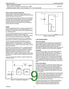
XTAL1 and XTAL2 are the input and output, respectively, of an
inverting amplifier. The pins can be configured for use as an on-chip
oscillator, as shown in the logic symbol.
V
DD
To drive the device from an external clock source, XTAL1 should be
driven while XTAL2 is left unconnected. There are no requirements
on the duty cycle of the external clock signal, because the input to
the internal clock circuitry is through a divide-by-two flip-flop.
However, minimum and maximum high and low times specified in
the data sheet must be observed.
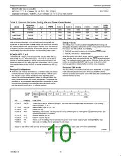
+
2.2 µF
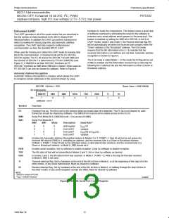
8XC552
RST
R
RST
RESET
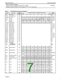
A reset is accomplished by either (1) externally holding the RST pin
high for at least two machine cycles (24 oscillator periods) or (2)
internally by an on-chip power-on detect (POD) circuit which detects
V
CC
ramping up from 0V.
To insure a good external power-on reset, the RST pin must be high
long enough for the oscillator to start up (normally a few
SU01114
milliseconds) plus two machine cycles. The voltage on V and the
RST pin must come up at the same time for a proper startup.
DD
Figure 2. Power-On Reset
For a successful internal power-on reset, the V voltage must
CC
ramp up from 0V smoothly at a ramp rate greater than 5V/100 ms.
LOW POWER MODES
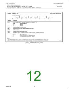
The RST line can also be pulled HIGH internally by a pull-up
transistor activated by the watchdog timer T3. The length of the
output pulse from T3 is 3 machine cycles. A pulse of such short
duration is necessary in order to recover from a processor or system
fault as fast as possible.
Stop Clock Mode
The static design enables the clock speed to be reduced down to
0 MHz (stopped). When the oscillator is stopped, the RAM and
Special Function Registers retain their values. This mode allows
step-by-step utilization and permits reduced system power
consumption by lowering the clock frequency down to any value. For
lowest power consumption the Power Down mode is suggested.
Note that the short reset pulse from Timer T3 cannot discharge the
power-on reset capacitor (see Figure 2). Consequently, when the
watchdog timer is also used to set external devices, this capacitor
arrangement should not be connected to the RST pin, and a
different circuit should be used to perform the power-on reset
operation. A timer T3 overflow, if enabled, will force a reset condition
to the 8XC554 by an internal connection, independent of the level of
the RST pin.
Idle Mode
In the idle mode (see Table 2), the CPU puts itself to sleep while
some of the on-chip peripherals stay active. The instruction to
invoke the idle mode is the last instruction executed in the normal
operating mode before the idle mode is activated. The CPU
contents, the on-chip RAM, and all of the special function registers
remain intact during this mode. The idle mode can be terminated
either by any enabled interrupt (at which time the process is picked
up at the interrupt service routine and continued), or by a hardware
reset which starts the processor in the same manner as a power-on
reset.
A reset may be performed in software by setting the software reset
bit, SRST (AUXR1.5).
V
DD
Power-Down Mode
To save even more power, a Power Down mode (see Table 2) can
be invoked by software. In this mode, the oscillator is stopped and
the instruction that invoked Power Down is the last instruction
executed. The on-chip RAM and Special Function Registers retain
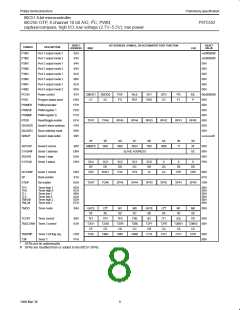
OVERFLOW
TIMER T3
SCHMITT
TRIGGER
their values down to 2.0V and care must be taken to return V to
CC
the minimum specified operating voltages before the Power Down
Mode is terminated.
RESET
CIRCUITRY
RST
Either a hardware reset or external interrupt can be used to exit from
Power Down. The Wake-up from Power-down bit, WUPD (AUXR1.3)
must be set in order for an external interrupt to cause a wake-up
from power-down. Reset redefines all the SFRs but does not
change the on-chip RAM. An external interrupt allows both the SFRs
and the on-chip RAM to retain their values.
ON-CHIP
RESISTOR
R
RST
SU00952
Figure 1. On-Chip Reset Configuration
To properly terminate Power Down the reset or external interrupt
should not be executed before V is restored to its normal
CC
operating level and must be held active long enough for the
oscillator to restart and stabilize (normally less than 10ms).
9
1999 Mar 30

 NXP [ NXP ]