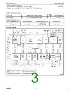
Philips Semiconductors
Preliminary specification
80C51 8-bit microcontroller
8K/256 OTP, 8 channel 10 bit A/D, I2C, PWM,
capture/compare, high I/O, low voltage (2.7V–5.5V), low power
P87C552
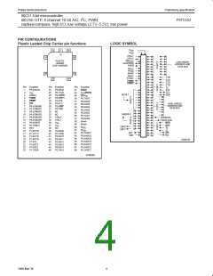
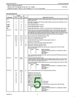
PIN DESCRIPTION
PIN NO.
MNEMONIC
PLCC
QFP
TYPE
NAME AND FUNCTION
V
DD
2
72
I
Digital Power Supply: Positive voltage power supply pin during normal operation, idle and
power-down mode.
STADC
3
74
I
Start ADC Operation: Input starting analog to digital conversion (ADC operation can also
be started by software).
PWM0
PWM1
EW
4
5
75
76
O
O
Pulse Width Modulation: Output 0.
Pulse Width Modulation: Output 1.
6
77
I
Enable Watchdog Timer: Enable for T3 watchdog timer and disable power-down mode.
P0.0-P0.7
57-50
58-51
I/O
Port 0: Port 0 is an 8-bit open-drain bidirectional I/O port. Port 0 pins that have 1s written
to them float and can be used as high-impedance inputs. Port 0 is also the multiplexed
low-order address and data bus during accesses to external program and data memory. In
this application it uses strong internal pull-ups when emitting 1s. Port 0 is also used to input
the code byte during programming and to output the code byte during verification.
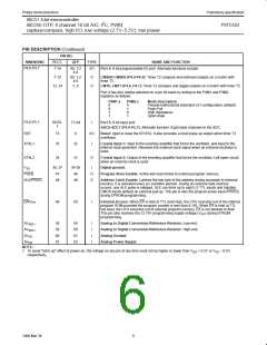
P1.0-P1.7
16-23
16-21
22-23
16-19
20
10-17
10-15
16-17
10-13
14
I/O
I/O
I/O
I
Port 1: 8-bit I/O port. Alternate functions include:
(P1.0-P1.5): Programmable I/O port pins.
(P1.6, P1.7): Open drain port pins.
CT0I-CT3I (P1.0-P1.3): Capture timer input signals for timer T2.
T2 (P1.4): T2 event input.
I
21
15
I
RT2 (P1.5): T2 timer reset signal. Rising edge triggered.
2
22
16
I/O
I/O
SCL (P1.6): Serial port clock line I C-bus.
2
23
17
SDA (P1.7): Serial port data line I C-bus.
Port 1 has four modes selected on a per bit basis by writing to the P1M1 and P1M2
registers as follows:
P1M1.x
P1M2.x
Mode Description
0
0
1
1
0
1
0
1
Pseudo–bidirectional (standard c51 configuration; default)
Push-Pull
High impedance
Open drain
Port 1 is also used to input the lower order address byte during EPROM programming and
verification. A0 is on P1.0, etc.
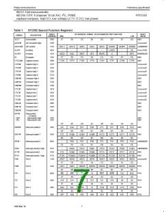
P2.0-P2.7
39-46
38-42,
45-47
I/O
Port 2: 8-bit programmable I/O port.
Alternate function: High-order address byte for external memory (A08-A15). Port 2 is also
used to input the upper order address during EPROM programming and verification. A8 is
on P2.0, A9 on P2.1, through A12 on P2.4.
Port 2 has four output modes selected on a per bit basis by writing to the P2M1 and P2M2
registers as follows:
P2M1.x
P2M2.x
Mode Description
0
0
1
1
0
1
0
1
Pseudo–bidirectional (standard c51 configuration; default)
Push-Pull
High impedance
Open drain
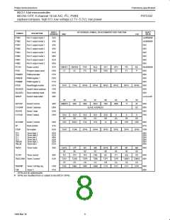
P3.0-P3.7
24-31
18-20,
23-27
I/O
Port 3: 8-bit programmable I/O port. Alternate functions include:
24
25
26
27
28
29
30
31
18
19
20
23
24
25
26
27
RxD(P3.0): Serial input port.
TxD (P3.1): Serial output port.
INT0 (P3.2): External interrupt.
INT1 (P3.3): External interrupt.
T0 (P3.4): Timer 0 external input.
T1 (P3.5): Timer 1 external input.
WR (P3.6): External data memory write strobe.
RD (P3.7): External data memory read strobe.
Port 3 has four modes selected on a per bit basis by writing to the P3M1 and P3M2
registers as follows:
P3M1.x
P3M2.x
Mode Description
0
0
1
1
0
1
0
1
Pseudo–bidirectional (standard c51 configuration; default)
Push–Pull
High impedance
Open drain
5
1999 Mar 30

 NXP [ NXP ]