Philips Semiconductors
Preliminary specification
80C51 8-bit microcontroller
8K/256 OTP, 8 channel 10 bit A/D, I2C, PWM,
capture/compare, high I/O, low voltage (2.7V–5.5V), low power
P87C552
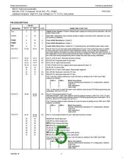
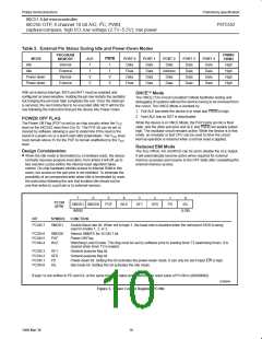
PIN DESCRIPTION (Continued)
PIN NO.
MNEMONIC
PLCC
QFP
TYPE
NAME AND FUNCTION
P4.0-P4.7
7-14
80, 1-2
4-8
I/O
Port 4: 8-bit programmable I/O port. Alternate functions include:
7-12
80, 1-2
4-6
O
O
CMSR0-CMSR5 (P4.0-P4.5): Timer T2 compare and set/reset outputs on a match with
timer T2.
13, 14
7, 8
CMT0, CMT1 (P4.6, P4.7): Timer T2 compare and toggle outputs on a match with timer T2.
Port 4 has four modes selected on a per bit basis by writing to the P4M1 and P4M2
registers as follows:
P4M1.x
P4M2.x
Mode Description
0
0
1
1
0
1
0
1
Pseudo-bidirectional (standard c51 configuration; default)
Push-Pull
High impedance
Open drain
P5.0-P5.7
68-62,
1
71-64
I
Port 5: 8-bit input port.
ADC0-ADC7 (P5.0-P5.7): Alternate function: Eight input channels to the ADC.
RST
15
35
9
I/O
I
Reset: Input to reset the 87C552. It also provides a reset pulse as output when timer T3
overflows.
XTAL1
32
Crystal Input 1: Input to the inverting amplifier that forms the oscillator, and input to the
internal clock generator. Receives the external clock signal when an external oscillator is
used.
XTAL2
34
31
O
Crystal Input 2: Output of the inverting amplifier that forms the oscillator. Left open-circuit
when an external clock is used.
V
36, 37
47
34-36
48
I
Digital ground.
SS
PSEN
O
O
Program Store Enable: Active-low read strobe to external program memory.
ALE/PROG
48
49
Address Latch Enable: Latches the low byte of the address during accesses to external
memory. It is activated every six oscillator periods. During an external data memory
access, one ALE pulse is skipped. ALE can drive up to eight LS TTL inputs and handles
CMOS inputs without an external pull-up. This pin is also the program pulse input (PROG)
during EPROM programming.
EA/V
49
50
I
External Access: When EA is held at TTL level high, the CPU executes out of the internal
program ROM provided the program counter is less than 8,192. When EA is held at TTL
low level, the CPU executes out of external program memory. EA is not allowed to float.
PP
This pin also receives the 12.75V programming supply voltage (V ) during EPROM
PP
programming.
AV
AV
AV
AV
58
59
60
61
59
60
61
63
I
I
I
I
Analog to Digital Conversion Reference Resistor: Low-end.
Analog to Digital Conversion Reference Resistor: High-end.
Analog Ground
REF–
REF+
SS
Analog Power Supply
DD
NOTE:
1. To avoid “latch-up” effect at power-on, the voltage on any pin at any time must not be higher or lower than V + 0.5V or V – 0.5V,
DD
SS
respectively.
6
1999 Mar 30

 NXP [ NXP ]