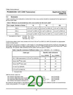
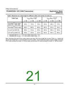
Philips Semiconductors
PCA82C250 / 251 CAN Transceiver
Application Note
AN96116
1
n – 1
V
= V
+ 2 × R × V ×
diff.in
+
(15)
------ -----------
diff.out
diff.in
W
R
R
T
diff
Equation (8) on page 17 is derived from equation (15).
APPENDIX 3 CALCULATION OF THE MAXIMUM BUS LINE LENGTH
Under worst case conditions the minimum differential input voltage of a dominant level at the receiving node must
be higher than the sum of the worst case switching threshold of the input transistor and a certain safety margin,
which is requested in the system. The requested input voltage was given by equation (9) on page 18. The worst
case value is given by
V
= V
+ k × (V
– V
)
with k = 0....1 .
sm
diff.in.req
th.max
sm
diff.out.min
th.max
Thus the relation (10) on page 19 is changed to
V
diff.out.min
V
=
≥ V
+ k × (V
– V )
th.max
.
(16)
-------------------------------------------------------------------------------------------
diff.in.min
th.max
sm
diff.out.min
n
– 1
1
max
1 + 2R
×
+
----------------- ---------------------
W.max
R
R
diff.min
T.min
With the definition
= ρ
R
× L
W.max
max
max
the maximum wiring length is determined using equation (16):
R
× R
diff.min
V
1
T.min
diff.out.min
----------------------
-------------------------------------------------------------------------
L
≤
× --------------------------------------------------------------------------------------------------------- – 1 ×
max
2 × ρ
R
+ (n
– 1)R
max T.min
V
+ k × (V
– V
)
th.max
max
diff.min
th.max
sm
diff.out.min
28

 NXP [ NXP ]