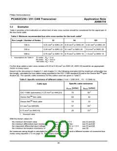
Philips Semiconductors
PCA82C250 / 251 CAN Transceiver
Application Note
AN96116
APPENDIX 1 ABBREVIATIONS AND DEFINITIONS
SR
single-ended slew rate of the signal transition at CANL and/or CANH
k
single-ended slew rate constant (in slope control mode the slew rate is pro-
portional to the current out of pin Rs of the transceiver)
SE
I
,
I
, I
Rs.min Rs.max
current (minimum, maximum) at pin Rs of the transceiver
typical voltage at pin Rs of the transceiver
Rs
V
P
V
Rs
x,y
OL
digital output port pin of a controller IC for transceiver mode control
nominal (maximum) LOW-level output voltage of the controller output port
,
V
OL.max
R
,
R
, R
nominal (minimum, maximum) value of the slope-control resistor at pin Rs
of the transceiver. This value determines the current and thus the slew rate
at CANL and CANH
ext
ext.min
ext.max
V
,
V
, V
nominal (minimum, maximum) value of the transceiver supply voltage
effective transceiver (other components) loop delay
CC
CC.min
CC.max
t
, t
loop.eff loop.eff.oth
∆t
difference between the effective loop delay of the transceiver in slope con-
trol mode and in high-speed mode
loop.eff
t
available two-way propagation delay (limited by CAN bit timing parame-
ters)
prop
t
t
specific line delay per length unit (e.g. 5 ns/m)
p
, t
loop delay of the transceiver between pin TxD (transmit data input) and
RxD (receive data output) at switching from recessive to dominant (domi-
nant to recessive) state (see [1] and [2])
onRxD
offRxD
t
length of the propagation segment of the bit period i.e. length of segment 1
(TSEG1) minus length of the resynchronization jump width (SJW)
PROPSEG
V
V
, V
, V
diff.in.req
nominal (minimum, requested) differential input voltage for reception
nominal (minimum) differential output voltage at the transmitting node
diff.in
diff.in.min
, V
V
diff.out
diff.out.min
th.max
V ,
nominal (maximum) differential input threshold voltage for detection of a
dominant bus condition
th
k
a factor indicating the safety margin for the differential input voltage for
sm
detecting a dominant bit at reception (0 < k
< 1)
sm
R
,
R
nominal (minimum) differential input resistance of a bus node in recessive
state (TxD = HIGH)
diff
diff.min
n,
R ,
n
number (maximum number) of bus nodes in the network
nominal (minimum) value for the bus termination resistors
nominal (maximum) series resistance of the bus wires
length (maximum length) of the bus wires between any two bus nodes
length of the unterminated cable stub.
max
R
T
T.min
W.max
max
R ,
R
W
L,
L
L
u
ρ,
R ,
ρ
, ρ
specific (typical, maximum) resistance per length unit of the bus wires
typ max
R
total (minimum total) differential resistive bus load as seen by the transmit-
ting node
L
L.min
26

 NXP [ NXP ]