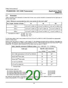
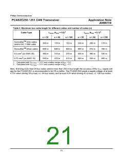
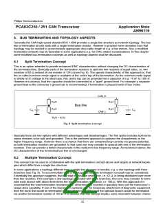
Philips Semiconductors
PCA82C250 / 251 CAN Transceiver
Application Note
AN96116
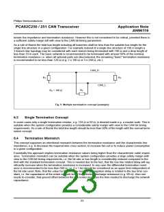
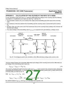
APPENDIX 2 CALCULATION OF THE VOLTAGE AT THE INPUT OF A NODE
For the calculation of the worst case (i.e. minimum) differential input voltage at the receiving node the following
assumptions or simplifications are made (see also Fig. 7 and Fig. 10):
• The termination resistors (R ) are located at the output of the transmitting and at the input of the receiving
T
node.
• The resistance of the lines between the transmitting and the receiving node is represented by the resistors
R .
W
• All other nodes are at the same end of the transmission line as the receiving node resulting in the minimum dif-
ferential input voltage.
• The output voltage of the transmitting node (V
) is supposed to be generated by a voltage source.
diff.out
output of
input of
transmitting
node (1)
receiving
node (n)
node inputs
(2...n-1)
bus wiring
termination
termination
I
W
R
W
R
(n-2)
diff
R
V
R
T
R
diff.out
diff
T
V
diff.in
I
I
T1
in
I
I
T2
in(n-2)
R
W
I
W
Fig. 10 Circuit diagram used for the calculation of the differential input voltage at the receiver node.
Thus the relation between the achievable differential input voltage at the receiving node and the differential out-
put voltage of the transmitting node is given by:
V
= V
+ 2 × R × I
W
(14)
diff.out
diff.in
W
The current I flowing through the bus lines splits up in I
(input current of the connected nodes without the
in(n-2)
W
transmitting and receiving one), I (current flowing through the termination resistor) and I (input current of the
T2
in
receiving node) as shown in Fig. 10.
With
I
= I
+ I + I
in
and
W
in(n – 2)
T2
R
diff
V
= I
× ----------- and V
= I × R
and V
= I × R
diff.in in diff
diff.in
in(n – 2)
diff.in
T2
T
n – 2
the relation between V
and V
is calculated from equation (14)
27
diff.out
diff.in

 NXP [ NXP ]