Philips Semiconductors
PCA82C250 / 251 CAN Transceiver
Application Note
AN96116
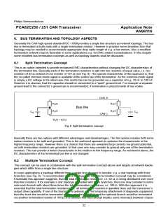
node
1
node
2
node
3
node
n
R
R
T
T
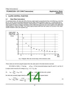
Fig. 6 Basic setup of a bus system (ISO 11898)
input of
receiving
node (#n)
output of
transmitting
node (#1)
node inputs
(#2 to #n-1)
termination
bus wiring
termination
R
W
CAN_H
R
(n-2)
diff
V
R
V
R
R
diff.out
T
diff.in
T
diff
CAN_L
R
W
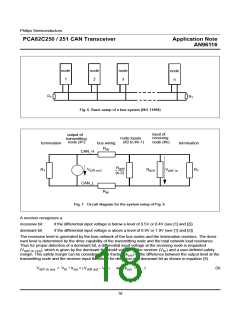
Fig. 7 Circuit diagram for the system setup of Fig. 6
A receiver recognizes a
recessive bit
dominant bit
if the differential input voltage is below a level of 0.5V or 0.4V (see [1] and [2])
if the differential input voltage is above a level of 0.9V or 1.0V (see [1] and [2])
The recessive level is generated by the bias network of the bus nodes and the termination resistors. The domi-
nant level is determined by the drive capability of the transmitting node and the total network load resistance.
Thus for proper detection of a dominant bit, a differential input voltage at the receiving node is requested
(V
), which is given by the dominant threshold voltage of the receiver (V ) and a user-defined safety
diff.in.req
th
margin. This safety margin can be considered as a fraction (k ) of the difference between the output level at the
sm
transmitting node and the receiver input threshold for detection of a dominant bit as shown in equation (9).
V
= V + k × (V
– V
)
with k = 0....1
sm
(9)
diff.in.req
th
sm
diff.out
th
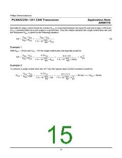
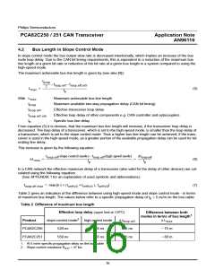
18

 NXP [ NXP ]