P82B715
NXP Semiconductors
I2C-bus extender
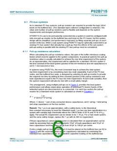
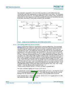
This equivalent capacitance is the sum of the capacitance on the buffered bus plus
10 times the sum of the capacitances on all the connected I2C-bus nodes. The calculated
value should not exceed 4 nF. The single buffered bus pull-up resistor is then calculated to
achieve the rise time requirement and it then provides the pull-up for the buffered bus and
for all other connected I2C-bus nodes included in the calculation.
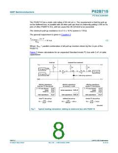
V
CC
= 5 V
R1
R2
R3
Sx
Sy
Lx
Ly
Lx
Ly
Sx
Sy
SDA
SCL
SDA
SCL
buffered bus
2
2
I C-bus 1
I C-bus 2
V
= 5 V
CC
R4
Lx
Ly
Sx
Sy
SDA
SCL
2
I C-bus 3
002aad691
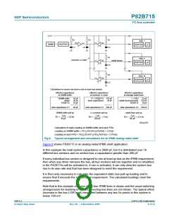
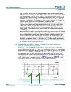
Fig 6. Single pull-up on buffered bus and multiple pull-up option
8.1.2 Calculating static bus drive currents
Figure 6 shows three P82B715s connected to a common buffered bus. The associated
bus capacitances are omitted for clarity and we assume the pull-up resistors have been
selected to give RC products equal to the bus rise time requirement. An I2C-bus chip
connected at I2C-bus 1 and holding the SDA bus LOW must sink the current flowing in its
local pull-up R1 plus, with assistance from the P82B715, the currents in R2, R3 and R4.
When I2C-bus 1 is LOW, the resistors R3 and R4 act to pull the bus nodes I2C-bus 2 and
I2C-bus 3, and their corresponding Sx pins, to a voltage higher than the voltage at their Lx
pins (which are LOW) so their buffer amplifiers will be inactive. The SDA at Sx of I2C-bus 2
and I2C-bus 3 is pulled LOW by the LOW at Lx via the internal 30 Ω resistor that links Lx
to Sx. So the effective current that must be sunk by the P82B715 buffer on I2C-bus 1, at its
Lx pin, is the sum of the currents in R2, R3 and R4. The Sx current that must be sunk by
an I2C-bus chip at I2C-bus 1, due to the buffer gain action, is 1⁄10 of the Lx current. So the
effective pull-up, determining the current to be sunk by an I2C-bus chip at I2C-bus 1, is R1
in parallel with resistors 10 times the values of R2, R3 and R4. If R1 = R3 = R4 = 10 kΩ,
and R2 = 1 kΩ, the effective pull-up load at I2C-bus 1 is
10 kΩ || 10 kΩ || 100 kΩ || 100 kΩ = 4.55 kΩ. (‘||’ means ‘in parallel with’.)
The same calculation applies for I2C-bus 2 or I2C-bus 3.
To calculate the current sunk by the Lx pin of the buffer at I2C-bus 1, note that the current
in R1 is sunk directly by the IC at I2C-bus 1. The buffer therefore sinks only the currents
flowing in R2, R3, and R4 so the effective pull-up is R2 in parallel with R3 and R4.
In this example that is 1 kΩ || 10 kΩ || 10 kΩ = 833 Ω. For a 5.5 V supply and 0.4 V LOW,
that means the buffer is sinking 16.3 mA.
P82B715_8
© NXP B.V. 2009. All rights reserved.
Product data sheet
Rev. 08 — 9 November 2009
7 of 23

 NXP [ NXP ]