P82B715
NXP Semiconductors
I2C-bus extender
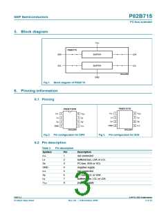
5. Block diagram
V
CC
P82B715
SDA
SCL
BUFFER
BUFFER
GND
LDA
LCL
002aad689
Fig 1. Block diagram of P82B715
6. Pinning information
6.1 Pinning
P82B715TD
P82B715PN
1
2
3
4
8
7
6
5
n.c.
Lx
V
CC
1
2
3
4
8
7
6
5
n.c.
Lx
V
CC
Ly
Ly
Sx
Sy
n.c.
Sx
Sy
n.c.
GND
GND
002aad686
002aad687
Fig 2. Pin configuration for DIP8
Fig 3. Pin configuration for SO8
6.2 Pin description
Table 3.
Pin description
Symbol
n.c.
Lx
Pin
1
Description
not connected
2
buffered bus, LDA or LCL
I2C-bus, SDA or SCL
negative supply
Sx
3
GND
n.c.
Sy
4
5
not connected
6
I2C-bus, SCL or SDA
buffered bus, LCL or LDA
positive supply
Ly
7
VCC
8
P82B715_8
© NXP B.V. 2009. All rights reserved.
Product data sheet
Rev. 08 — 9 November 2009
3 of 23

 NXP [ NXP ]