P82B715
NXP Semiconductors
I2C-bus extender
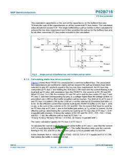
• The 300 ns bus fall time, and the Standard-mode I2C-bus limit specification limit of
400 pF, must also be observed. If the 400 pF limit is observed the fall time limit will be
met. Allocate about 1⁄3 of this 400 pF limit, or 133 pF, to each I2C-bus leaving 2⁄3, or
266 pF, for the cable bus loading as it will appear at the Sx/Sy pins. The ×10 gain of
P82B715 allows the loading at Lx/Ly to be 10 times the load at Sx/Sy, so 2660 pF
maximum. The loading at Lx/Ly due to the other standard buses is 133 pF each. For
just one remote module the cable capacitance may then be up to
(2660 − 133) = 2530 pF. For typical twisted pair or flat cables, as used for telephony or
Ethernet (Cat5e) wiring, that capacitance is around 50 pF to 70 pF / meter so the
cable could, in theory, be up to 50 m long. From practical experience, 30 m has
proven a safe cable length to be driven in this simple way, up to 100 kHz, with the
values shown. Longer distances and higher speeds are possible but require more
careful design.
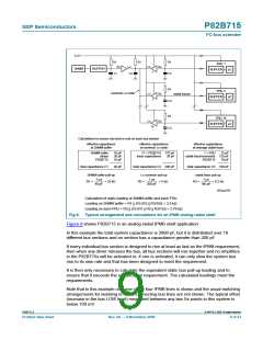
• If there are severe EMI/ESD tests to be passed then large clamp diodes can be fitted
on the cable bus at each module to VCC and to ground. They may be diodes rated for
this ESD application, or simply large rectifiers (1N4000). The low-impedance bus
easily accommodates their relatively large capacitance. The P82B715 does not
provide any isolation between Lx and Sx, so this clamping method provides the best
protection for the lower voltage I2C-bus parts. The VCC supply should be bypassed
using low-impedance capacitors. Zeners may be fitted to prevent the supply rising due
to rectification during very large interference.
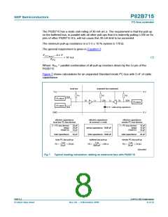
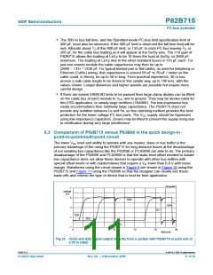
8.3 Comparison of P82B715 versus P82B96 in the quick design-in
point-to-point/multi-point circuit
The lower VOL level and ability to operate with any master, slave or bus buffer is the
primary advantage of the using the P82B715 for long distance buses at the disadvantage
of not isolating bus capacitance like the P82B96 or PCA9600 are able to do. The primary
disadvantage of the P82B96 and PCA9600 is that the static level offset needed to isolate
bus capacitance does not allow these devices to operate with other bus buffers with
special offset levels or with master/slaves that require a VIL lower than 0.8 V with noise
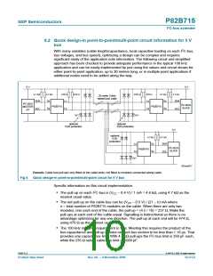
margin. Waveforms using the circuit shown in Figure 9 are shown in Figure 10 using the
P82B715 and Figure 11 using the P82B96 so that the designer can clearly see these
trade-offs and choose the type of device that is best for their application.
002aad818
7
voltage
(V)
5
SDA
SDA
3
SCL
SDA
1
SCL
SCL
−1
0
4
8
12
16
20
time (µs)
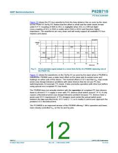
Fig 10. Clock and data signal output at Sx/Sy from a system with P82B715 at each end of
a 20 m cable
P82B715_8
© NXP B.V. 2009. All rights reserved.
Product data sheet
Rev. 08 — 9 November 2009
11 of 23

 NXP [ NXP ]