P82B715
NXP Semiconductors
I2C-bus extender
8.1 I2C-bus systems
As in standard I2C-bus systems, pull-up resistors are required to provide the logic HIGH
levels on the buffered bus. (The standard open-collector configuration is retained.) The
value and number of pull-up resistors used is flexible and depends on the system
requirements and designer preferences.
If P82B715 ICs are to be permanently connected into a system it could be configured with
only one pull-up resistor on the buffered bus and none on the I2C-buses, but the system
design will be simplified, and performance improved, by fitting separate pull-ups on each
section of the bus. When a sub-system using P82B715 may be optionally connected to an
existing I2C-bus system that already has a pull-up, then the effects of the sub-system
pull-ups acting in parallel with the existing I2C-bus pull-up must be considered.
8.1.1 Pull-up resistance calculation
When calculating the pull-up resistance values, the gain of the buffer introduces scaling
factors which must be applied to the system components. In practical systems the pull-up
resistance value is usually calculated to achieve the rise time requirement of the system.
As an approximation, this requirement will be satisfied for a standard 100 kHz system if
the time constant of the total system (product of the net resistance and net capacitance) is
set to 1 microsecond or less.
In systems using P82B715s, the most convenient way to achieve the total system
rise time requirement is by considering each bus node separately. Each of the I2C-bus
nodes, and the buffered bus node, is designed by selecting its pull-up resistor to provide
the required rise time by setting its time constant (product of the pull-up resistance and
load capacitance) equal to the I2C-bus rise time requirement. If each node complies, then
the system requirement will also be met with a small safety margin.
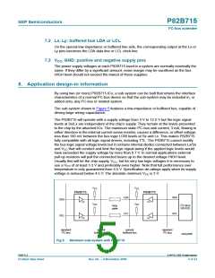
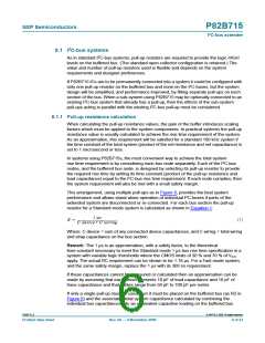
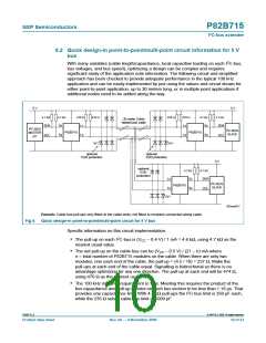
This arrangement, using multiple pull-ups as in Figure 6, provides the best system
performance and allows stand-alone operation of individual I2C-buses if parts of the
extended system are disconnected or re-connected. For each bus section the pull-up
resistor for a Standard-mode system is calculated as shown in Equation 1:
1 µs
R =
(1)
-----------------------------------------------------
C device + C wiring
Where: C device = sum of any connected device capacitances, and C wiring = total wiring
and stray capacitance on the bus section.
Remark: The 1 µs is an approximation, with a safety factor, to the theoretical
time-constant necessary to meet the Standard-mode 1 µs bus rise time specification in a
system with variable logic thresholds where the CMOS limits of 30 % and 70 % of VCC
apply. The actual RC requirement can be shown to be 1.18 µs. For a Fast-mode system,
and the same safety margin, replace the 1 µs with its 300 ns requirement.
If these capacitances cannot be measured or calculated then an approximation can be
made by assuming that each device presents 10 pF of load capacitance and 10 pF of
trace capacitance and that cables range from 50 pF to 100 pF per meter.
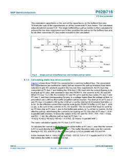
If only a single pull-up must be used then it must be placed on the buffered bus (as R2 in
Figure 6) and the associated total system capacitance calculated by combining the
individual bus capacitances into an equivalent capacitive loading on the buffered bus.
P82B715_8
© NXP B.V. 2009. All rights reserved.
Product data sheet
Rev. 08 — 9 November 2009
6 of 23

 NXP [ NXP ]