P82B715
NXP Semiconductors
I2C-bus extender
7. Functional description
The P82B715 is a dual bidirectional logic signal device having unity voltage gain in both
directions, but ×10 current amplification in one direction that allows increasing the
allowable I2C-bus system capacitance. It contains identical circuits for each I2C-bus signal
and requires no external directional control. It uses unidirectional analog current
amplification to increase the current sink capability of I2C-bus chips by a factor of 10 and
to change the I2C-bus specification limit of 400 pF to a 4 nF system limit. This allows
I2C-bus, or similar bus systems, to be extended over long distances using conventional
cables and without degradation of system performance.
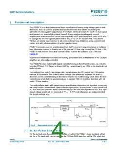
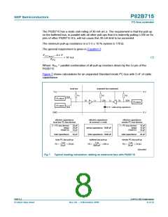
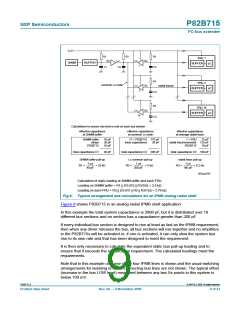
P82B715 provides current amplification from its I2C-bus to its low-impedance or buffered
bus. Whenever current is flowing out of Sx, into an I2C-bus chip driving the I2C-bus LOW,
P82B715 will sink ten times that current into Lx to drive the buffered bus LOW (see
Figure 4).
To minimize interference and ensure stability, the current rise and fall times of the Lx drive
amplifier are internally controlled.
The P82B715 does not amplify signal currents flowing in the other direction, i.e., into Sx
from the I2C-bus. The Sx pin is driven LOW by current flowing out of Lx to the driver of that
buffered side.
The buffered bus logic LOW voltage at Lx simply drives the I2C-bus at Sx LOW via the
internal 30 Ω resistor. The buffer’s offset voltage (the difference between Sx and Lx)
depends on the current flowing in the sense resistor so it will be very small when the bus
currents are small, but it is guaranteed not to exceed 100 mV in either direction with full
static I2C-bus loading.
The unity voltage gain, with signal current amplification dependent on direction, preserves
the multi-master, bidirectional, open-collector/open-drain, characteristic of any connected
I2C-bus lines and provides these characteristics to the new low-impedance bus. Bus logic
signal voltage levels will be clamped at (VCC + 0.7 V), but otherwise are independent of
the supply voltage VCC
.
I
= I
Lx
Sx
I
I
Sx
I
= 10 × I
Sx
Sx
Lx
CURRENT
SENSE
2
Lx buffered bus
I C-bus Sx
9 × I
Sx
30 Ω
V
CC
GND
002aad688
Fig 4. Equivalent circuit: one-half P82B715
7.1 Sx, Sy: I2C-bus SDA or SCL
On the normal side, because the two buffer circuits in the P82B715 are identical, either
the Sx or Sy input pins can be used as the I2C-bus SDA data line, or the SCL clock line.
P82B715_8
© NXP B.V. 2009. All rights reserved.
Product data sheet
Rev. 08 — 9 November 2009
4 of 23

 NXP [ NXP ]