P82B715
NXP Semiconductors
I2C-bus extender
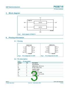
7.2 Lx, Ly: buffered bus LDA or LCL
On the special low-impedance or buffered line side, the corresponding output at the Lx or
Ly pins becomes the LDA data line or LCL clock line.
7.3 VCC, GND: positive and negative supply pins
The power supply voltages at each P82B715 used in a system are normally nominally the
same. If they differ by a significant amount, noise margin may be sacrificed as the bus
HIGH level should not exceed the lowest of those supplies.
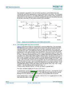
8. Application design-in information
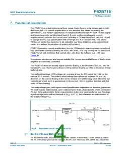
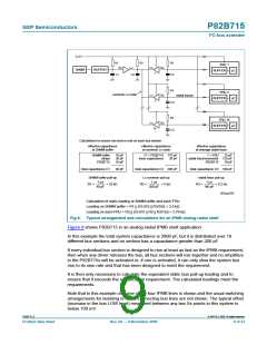
By using two (or more) P82B715 ICs, a sub-system can be built that retains the interface
characteristics of a normal I2C-bus device so that the sub-system may be included in, or
added onto, any I2C-bus or related system.
The sub-system shown in Figure 5 features a low-impedance or buffered bus, capable of
driving large wiring capacitance.
The P82B715 will operate with a supply voltage from 3 V to 12.5 V but the logic signal
levels at Sx/Lx are independent of the chip’s supply. They remain at the levels presented
to the chip by the attached ICs. The maximum static I2C-bus sink current, 3 mA, flowing in
either direction in the internal current sense resistor, causes a difference, or offset voltage,
less than 100 mV between the bus logic LOW levels at Sx and Lx. This makes P82B715
fully compatible with all logic signal drivers, including TTL. The P82B715 cannot modify
the bus logic signal voltage levels but it contains internal diodes connected between Lx/Sx
and VCC that will conduct and limit the logic signal swing if the applied logic levels would
have exceeded the supply voltage by more than 0.7 V. In normal applications external
pull-up resistors will pull the connected buses up to the desired voltage HIGH level.
Usually this will be the chip supply, VCC, but for very low logic voltages it is necessary to
use a VCC of at least 3.3 V and preferably even higher. Note that full performance over
temperature is only guaranteed from 4.5 V. Specification de-ratings apply when its supply
voltage is reduced below 4.5 V. The absolute minimum VCC is 3 V.
V
V
V
V
CC
CC
CC
CC
P82B715
P82B715
LDA
LCL
SDA
SCL
SDA
SCL
1/2
1/2
2
I C-BUS
long
cable
DEVICE
1/2
1/2
standard
I C-bus
special
buffered bus
special
buffered bus
standard
I C-bus
2
2
002aad690
Fig 5. Minimum sub-system with P82B715
P82B715_8
© NXP B.V. 2009. All rights reserved.
Product data sheet
Rev. 08 — 9 November 2009
5 of 23

 NXP [ NXP ]