KMA220
NXP Semiconductors
Dual channel programmable angle sensor
Table 18. Command byte bit description …continued
Bit
4 to 1
0
Symbol
CMD[4:1]
CMD0
Description
address bits
read/write
0 = write
1 = read
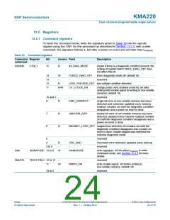
A more detailed description of all customer accessible registers is given in Section 13.5.
Both default value and the complete command including the address and write or read
request are also listed.
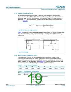
13.3.1 Write access
To write data to the non-volatile memory, enable the internal charge pump. Set bits
CP_CLOCK_EN and WRITE_EN and wait for tcp enables the internal charge pump.
Perform the following procedure for write access:
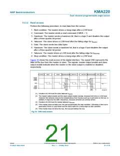
1. Start condition: The master drives a rising edge after a LOW level
2. Command: The master sends a write command (CMD0 = 0)
3. Data: The master sends two data bytes
4. Stop condition: The master drives a rising edge after a LOW level
Figure 15 shows the write access of the digital interface. The signal OWI represents the
data on the bus from the master or slave. The signals: master output enable and slave
output enable indicate when the master or the slave output is enabled or disabled,
respectively.
START
CMD7
CMD0
WDATA15
WDATA0
STOP
IDLE
master
output
enable
OWI
(2)
slave
output
enable
(1)
001aag743
(1) Missing rising edges generate a time-out condition and the written data is ignored.
(2) If the master does not drive the bus, the bus-pull defines the bus.
Fig 15. OWI write access
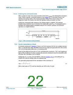
Note: As already mentioned in Section 13.1, use the write procedure to enter the
command mode. If command mode is not entered, communication is not possible and the
sensor operates in normal operation mode. After changing an address, the time tprog must
elapse before changing another address. After changing the contents of the non-volatile
memory, recalculate and write the checksum (see Section 13.4).
KMA220
All information provided in this document is subject to legal disclaimers.
© NXP B.V. 2012. All rights reserved.
Product data sheet
Rev. 1 — 24 May 2012
20 of 36

 NXP [ NXP ]