ISP1160
Embedded USB Host Controller
Philips Semiconductors
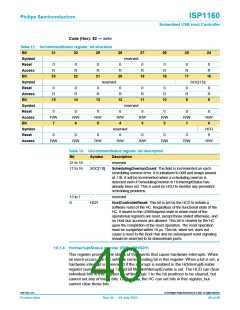
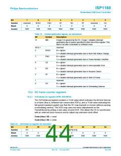
Bit
7
reserved
0
6
RHSC
0
5
4
UE
0
3
RD
0
2
SF
0
1
reserved
0
0
SO
0
Symbol
Reset
Access
FNO
0
R/W
R/W
R/W
R/W
R/W
R/W
R/W
R/W
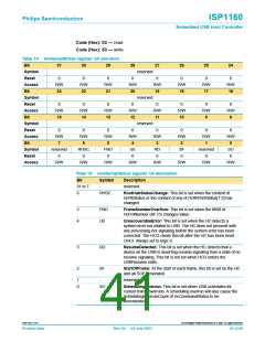
Table 19: HcInterruptDisable register: bit description
Bit
Symbol
Description
31
MIE
A logic 0 is ignored by the HC. A logic 1 disables interrupt
generation due to events specified in other bits of this register. This
field is set after a hardware or software reset.
30 to 7
6
-
reserved
RHSC
0 — ignore
1 — disable interrupt generation due to Root Hub Status Change
5
4
3
2
FNO
UE
0 — ignore
1 — disable interrupt generation due to Frame Number Overflow
0 — ignore
1 — disable interrupt generation due to Unrecoverable Error
RD
SF
0 — ignore
1 — disable interrupt generation due to Resume Detect
0 — ignore
1 — disable interrupt generation due to Start of Frame
1
0
-
reserved
SO
0 — ignore
1 — disable interrupt generation due to Scheduling Overrun
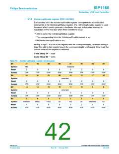
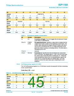
10.2 HC frame counter registers
10.2.1 HcFmInterval register (R/W: 0DH/8DH)
The HcFmInterval register contains a 14-bit value which indicates the bit time interval
in a frame (that is, between two consecutive SOFs), and a 15-bit value indicating the
full-speed maximum packet size that the HC may transmit or receive without causing
a scheduling overrun. The HCD may carry out minor adjustments on the
FrameInterval by writing a new value at each SOF. This allows the HC to synchronize
with an external clock resource and to adjust any unknown clock offset.
Code (Hex): 0D — read
Code (Hex): 8D — write
Table 20: HcFmInterval register: bit allocation
Bit
31
FIT
0
30
29
28
27
26
25
24
Symbol
Reset
Access
FSMPS[14:8]
0
0
0
0
0
0
0
R/W
R/W
R/W
R/W
R/W
R/W
R/W
R/W
9397 750 11371
© Koninklijke Philips Electronics N.V. 2003. All rights reserved.
Product data
Rev. 04 — 04 July 2003
44 of 88

 NXP [ NXP ]