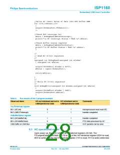
ISP1160
Embedded USB Host Controller
Philips Semiconductors
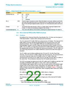
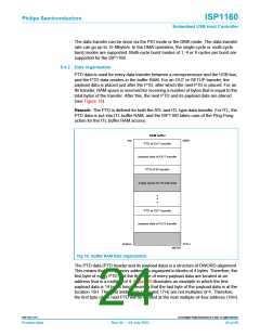
The data transfer can be done via the PIO mode or the DMA mode. The data transfer
rate can go up to 15 Mbyte/s. In the DMA operation, the single-cycle or multi-cycle
burst modes are supported. Multi-cycle burst modes of 1, 4 or 8 cycles per burst are
supported for the ISP1160.
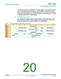
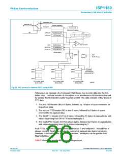
9.4.2 Data organization
PTD data is used for every data transfer between a microprocessor and the USB bus,
and the PTD data resides in the buffer RAM. For an OUT or SETUP transfer, the
payload data is placed just after the PTD, after which the next PTD is placed. For an
IN transfer, RAM space is reserved for receiving a number of bytes that is equal to the
total bytes of the transfer. After this, the next PTD and its payload data are placed
(see Figure 18).
Remark: The PTD is defined for both the ATL and ITL type data transfer. For ITL, the
PTD data is put into ITL buffer RAM, and the ISP1160 takes care of the Ping-Pong
action for the ITL buffer RAM access.
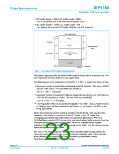
RAM buffer
top
000H
PTD of OUT transfer
payload data of OUT transfer
PTD of IN transfer
empty space for IN total data
PTD of OUT transfer
payload data of OUT transfer
bottom
7FFH
MGT952
Fig 18. Buffer RAM data organization.
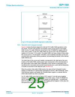
The PTD data (PTD header and its payload data) is a structure of DWORD alignment.
This means that the memory address is organized in blocks of 4 bytes. Therefore, the
first byte of every PTD and the first byte of every payload data are located at an
address that is a multiple of 4. Figure 19 illustrates an example in which the first
payload data is 14 bytes long, meaning that the last byte of the payload data is at the
location 15H. The next addresses (16H and 17H) are not multiples of 4. Therefore,
the first byte of the next PTD will be located at the next multiple-of-four address (18H).
9397 750 11371
© Koninklijke Philips Electronics N.V. 2003. All rights reserved.
Product data
Rev. 04 — 04 July 2003
24 of 88

 NXP [ NXP ]