RSL10
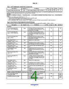
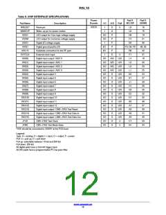
Table 3. ELECTRICAL PERFORMANCE SPECIFICATIONS
Unless otherwise noted, the specifications mentioned in the table below are valid at 25°C at VBAT = VDDO = 1.25 V.
Description
Symbol
Conditions
Min
Typ
Max
Units
FLASH SPECIFICATIONS
Endurance for sections NVR1,
NVR2, and NVR3 (6 kB in total)
1000
write/
erase
cycles
Retention
25
years
Product parametric performance is indicated in the Electrical Characteristics for the listed test conditions, unless otherwise noted. Product
performance may not be indicated by the Electrical Characteristics if operated under different conditions.
(ꢀꢁꢂꢃ)
ℴ∮׆
ᣩᛄ,“ꢆᷴሇ”ꢎꢁꢂꢃꢏ᠏ᐠꢂἫᚥꢄ⛻ꢏڡ
ሇ்ꢀᝐ。ꢄꢅई⛽
ꢄ⛻᪠ጜ,ڡ
ሇ்
்⛾“ꢆᷴሇ”ꢎ
ꢁᐠꢂሇ்ꢀᝐ⛽⛰ೄ。
2. The maximum VDDC voltage cannot exceed the VBAT input voltage or the VCC output from the buck converter.
3. The maximum VDDM voltage cannot exceed the VBAT input voltage or the VCC output from the buck converter.
4. The maximum VDDRF voltage cannot exceed the VBAT input voltage or the VCC output from the buck converter.
5. The VDDRF calibrated targets are:
− 1.10 V (TX power > 0 dBm, with optimal RX sensitivity)
− 1.07 V (TX power = 0 dBm)
− 1.20 V (TX power = 2 dBm)
The VDDPA calibrated targets are:
− 1.30 V
− 1.26 V (TX power = 3 dBm, assumes VDDRF = 1.10 V)
− 1.60 V (TX power = 6 dBm, assumes VDDRF = 1.10 V)
6. The LDO can be used to regulate down from VBAT and generate VCC. For VBAT values higher than 1.5 V, the LDO is less efficient and it
is possible to save power by activating the DC−DC converter to generate VCC.
7. Signal generated by RF tester.
8. 0.5 to 1.0 dB degradation in the RX sensitivity is present on the QFN package vs WLCSP. This is attributed to the presence of the metal slug
of the QFN package which is in close proximity to on−chip inductors.
9. All values are based on evaluation board performance at the antenna connector, including the harmonic filter loss
10.The values shown here are without RF filter. Harmonics need to be filtered with an external filter (See “RF Filter” on Table 6).
11. These specifications have been validated with the Epson Toyocom MC – 306 crystal
Table 4. VDDM Target Trimming Voltage in Function of VDDO Voltage
VDDM Voltage (V)
DIO_PAD_CFG DRIVE
Maximum VDDO Voltage (V)
1.05
1.05
1.10
1
0
0
2.7
3.2
3.2
Table 5. VDDM Target Trimming Voltage in Function of SYSCLK Frequency
VDDM Voltage (V)
Maximum SYSCLK Frequency (MHz)
Restriction
0.92
≤ 24
The ADC will be functional in low frequency
mode and between 0 and 85°C only.
1.00
1.05
≤ 24
Fully functional
Fully functional
48
www.onsemi.cn
8

 ONSEMI [ ONSEMI ]