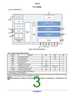
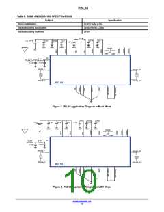
RSL10
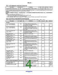
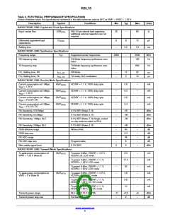
Table 3. ELECTRICAL PERFORMANCE SPECIFICATIONS
Unless otherwise noted, the specifications mentioned in the table below are valid at 25°C at VBAT = VDDO = 1.25 V.
Description
Symbol
Conditions
Min
Typ
Max
Units
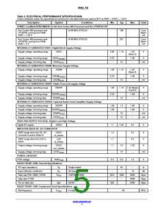
RADIO FRONT−END: Crystal and Clock Specifications
Equiv. series Res.
ESR
RSL10 has internal load capacitors,
additional external capacitors are not
required
20
−
80
W
XTAL
Differential equivalent load
capacitance
CL
6
8
10
pF
XTAL
Settling time
−
0.5
1.5
ms
RADIO FRONT−END: Synthesizer Specifications
Frequency range
RX frequency step
F
RF
Supported carrier frequencies
2360
−
−
2500
100
MHz
Hz
RX Mode frequency synthesizer reso-
lution
−
TX frequency step
TX Mode frequency synthesizer reso-
lution
−
−
600
Hz
PLL Settling time, RX
PLL Settling time, TX
t
RX Mode
−
−
15
5
25
10
ms
ms
PLL_RX
t
TX mode, BLE modulation
PLL_TX
RADIO FRONT−END: Receive Mode Specifications
Current consumption at 1 Mbps,
= 1.25 V
IBAT
IBAT
IBAT
IBAT
VDDRF = 1.1 V, 100% duty cycle
VDDRF = 1.1 V, 100% duty cycle
VDDRF = 1.1 V, 100% duty cycle
VDDRF = 1.1 V, 100% duty cycle
−
−
−
−
5.6
6.2
3.0
3.4
−
−
−
−
mA
mA
mA
mA
RFRX
RFRX
RFRX
RFRX
V
BAT
Current consumption at 2 Mbps,
= 1.25 V
V
BAT
Current consumption at 1 Mbps,
= 3 V, DC−DC
V
BAT
Current consumption at 2 Mbps,
= 3 V, DC−DC
V
BAT
RX Sensitivity, 0.25 Mbps
RX Sensitivity, 0.5 Mbps
RX Sensitivity, 1 Mbps, BLE
0.1% BER (Notes 7, 8)
0.1% BER (Notes 7, 8)
−
−
−
−97
−96
−94
−
−
−
dBm
dBm
dBm
0.1% BER (Notes 7, 8) Single−ended
on chip antenna match to 50 W
RX Sensitivity, 2 Mbps, BLE
RSSI effective range
RSSI step size
0.1% BER (Notes 7, 8)
Without AGC
−
−
−
−
−
0
−92
60
2.4
48
6
−
−
−
−
−
−
dBm
dB
dB
RX AGC range
dB
RX AGC step size
Max usable signal level
Programmable
0.1% BER
dB
5
dBm
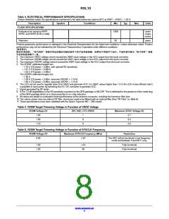
RADIO FRONT−END: Transmit Mode Specifications
Tx peak power consumption at
VBAT = 1.25 V (Note 9)
IBAT
Tx power 0 dBm, VDDRF = 1.07 V,
VDDPA: off, LDO mode
−
−
−
−
−
−
8.9
17.4
25
−
−
−
−
−
−
mA
mA
mA
mA
mA
mA
RFTX
Tx power 3 dBm, VDDRF = 1.1 V,
VDDPA = 1.26 V, LDO mode
Tx power 6 dBm, VDDRF = 1.1 V,
VDDPA = 1.60 V, LDO mode
Tx peak power consumption at
VBAT = 3 V (Note 9)
IBAT
Tx power 0 dBm, VDDRF = 1.07 V,
VDDPA: off, DC−DC mode
4.6
8.6
12
RFTX
Tx power 3 dBm, VDDRF = 1.1 V,
VDDPA = 1.26 V, DC−DC mode
Tx power 6 dBm, VDDRF = 1.1 V,
VDDPA = 1.60 V, DC−DC mode
Transmit power range
BLE or 802.15.4 OQPSK
Full band.
−17
+0.5
2
+6
dBm
dB
Transmit power step size
−
−
www.onsemi.cn
6

 ONSEMI [ ONSEMI ]