RSL10
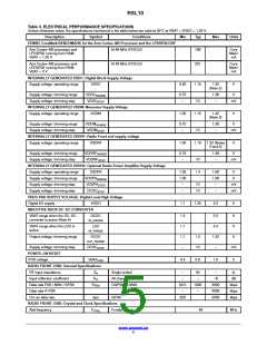
Table 3. ELECTRICAL PERFORMANCE SPECIFICATIONS
Unless otherwise noted, the specifications mentioned in the table below are valid at 25°C at VBAT = VDDO = 1.25 V.
Description
Symbol
Conditions
Min
Typ
Max
Units
RADIO FRONT−END: Transmit Mode Specifications
Transmit power accuracy
Tx power 3 dBm. Full band. Relative to
the typical value.
−1.5
−1.5
−
−
+1
dB
Tx power 0 dBm. Full band. Relative to
the typical value.
−
1.5
dB
nd
Power in 2 harmonic
0 dBm mode. 50 W for “Typ” value.
(Note 10)
−31
−40
−49
−18
−31
−42
dBm
dBm
dBm
rd
Power in 3 harmonic
0 dBm mode. 50 W for “Typ” value.
(Note 10)
−
th
Power in 4 harmonic
0 dBm mode. 50 W for “Typ” value.
(Note 10)
−
ADC
Resolution
ADC
8
0
12
−
14
2
bits
V
RES
Input voltage range
ADC
RANGE
INL
ADC
−2
−
+2
mV
mV
kHz
INL
DNL
DNL
ADC
−1
−
+1
Channel sampling frequency
ADC
For the 8 channels sequentially,
SLOWCLK = 1 MHz
0.0195
−
6.25
CH_SF
32 kHz ON−CHIP RC OSCILLATOR
Untrimmed Frequency
Trimming steps
Freq
20
2
32
50
5
kHz
%
UNTR
Steps
1.5
3 MHz ON−CHIP RC OSCILLATOR
Untrimmed Frequency
Trimming steps
Freq
3
MHz
%
UNTR
Steps
Fhi
1.5
10
Hi Speed mode
MHz
32 kHz ON−CHIP CRYSTAL OSCILLATOR (Note 11)
Output Frequency
Freq
Depends on xtal parameters
Steps of 0.4 pF
32768
1
Hz
s
32k
Startup time
3
Internal load trimming range
External load Capacitance
0
25.2
3.5
pF
pF
Maximum external capacity allowed
(package, routing, etc.)
ESR
100
60
kW
Duty Cycle
40
50
%
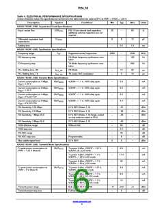
DC CHARACTERISTICS OF THE DIGITAL PADS − With VDDO = 2.97 V – 3.3 V, nominal: 3.0 V Logic
Voltage level for high input
Voltage level for low input
V
2
VDDO+0.3
0.8
V
V
IH
V
VSSD−
0.3
IL
DC CHARACTERISTICS OF THE DIGITAL PADS − With VDDO = 1.1 V – 1.32 V, nominal: 1.2 V Logic
Voltage level for high Input
V
0.65*
VDDO+0.3
V
V
IH
VDDO
Voltage level for low input
V
VSSD−
0.3
0.35* VDDO
IL
DIO DRIVE STRENGTH
DIO drive strength
IDIO
2
12
12
mA
FLASH SPECIFICATIONS
Endurance of the 384 kB of flash
100,000
write/
erase
cycles
www.onsemi.cn
7

 ONSEMI [ ONSEMI ]