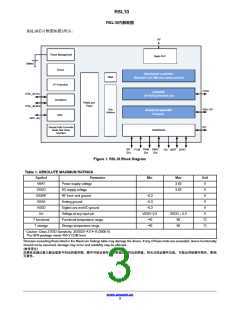
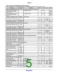
RSL10
RF
Power Management
Radio PHY
Battery
Timers
Baseband controller
Bluetooth 5 (LE 2M) and custom protocol
DMA
IP Protection
JTAG
LPDSP32
32−bit Dual Harvard core
XTAL_32 kHz
Oscillators
RAMs and
Flash
XTAL_48 MHz
SWJ−DP
Bus
Arbiters
Arm[ Cortex[-M3
Processor
ADC
ADC (4x)
I2C
Sample Rate Converter
Audio Sink Clock
Counters
Interfaces
SPI
(2x)
PCM PWM DMIC
(2x) (2x)
OD UART GPIO
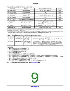
Figure 1. RSL10 Block Diagram
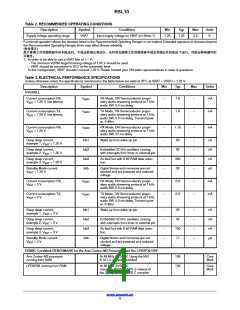
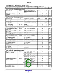
Table 1. ABSOLUTE MAXIMUM RATINGS
Symbol
VBAT
Parameter
Power supply voltage
Min
Max
3.63
3.63
Unit
V
VDDO
I/O supply voltage
V
VSSRF
VSSA
RF front−end ground
−0.3
−0.3
−0.3
V
Analog ground
V
VSSD
Digital core and I/O ground
Voltage at any input pin
Functional temperature range
Storage temperature range
V
Vin
VSSD−0.3
−40
VDDC + 0.3
V
T functional
T storage
85
85
°C
°C
−40
Caution: Class 2 ESD Sensitivity, JESD22−A114−B (2000 V)
The QFN package meets 450 V CDM level
Stresses exceeding those listed in the Maximum Ratings table may damage the device. If any of these limits are exceeded, device functionality
should not be assumed, damage may occur and reliability may be affected.
(ꢀꢁꢂꢃ)
ꢄꢅꢆꢇꢈꢉꢊꢋꢌꢍꢀꢎꢁꢂꢃꢏꢀꢐꢑ,ࡈ
ꢄ
்ꢅᔿय。ꢄꢅꢈꢉÛĵ᪩{℠ꢀ,෦ៀẵƽᚑࡈ
ꢄѿ்,
்ꢅොೄࡈ
ꢄᔿय,ᅑڭ
www.onsemi.cn
3

 ONSEMI [ ONSEMI ]