NCP3170
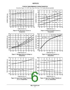
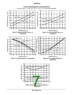
TYPICAL PERFORMANCE CHARACTERISTICS
(Circuit from Figure 1, T = 25°C, V = V = 12 V, V = 3.3 V unless otherwise specified)
A
IN
EN
OUT
130
120
110
40
35
30
25
Input Voltage = 4.5 V
100
90
Input Voltage = 4.5 V
Input Voltage = 12 V, 18 V
Input Voltage = 12 V, 18 V
80
20
15
70
60
−50 −30 −10
10
30
50
70
90 110 130
−50 −30 −10
10
30
50
70
90
110 130
TEMPERATURE (°C)
TEMPERATURE (°C)
Figure 15. High Side MOSFET RDS(on) vs.
Temperature
Figure 16. Low Side MOSFET RDS(on) vs.
Temperature
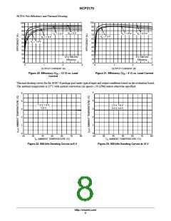
215
210
1001.5
1001.0
1000.5
1000.0
999.5
Input Voltage = 12 V
Input Voltage = 4.5 V
205
200
195
190
999.0
Input Voltage = 4.5 V
Input Voltage = 18 V
Input Voltage = 18 V
998.5
998.0
997.5
Input Voltage = 12 V
185
180
997.0
996.5
−50 −30 −10
10
30
50
70
90
110 130
−50 −30 −10
10
30
50
70
90
110 130
TEMPERATURE (°C)
TEMPERATURE (°C)
Figure 17. Transconductance vs. Temperature
Figure 18. Over Voltage Protection vs.
Temperature
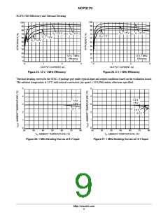
4.45
4.40
Input Under Voltage Protection Rising
4.35
4.30
4.25
4.20
4.15
Input Under Voltage Protection Falling
4.10
4.05
−50 −30 −10
10
30
50
70
90
110 130
TEMPERATURE (°C)
Figure 19. Input Under Voltage Protection vs.
Temperature
http://onsemi.com
7

 ONSEMI [ ONSEMI ]