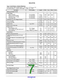
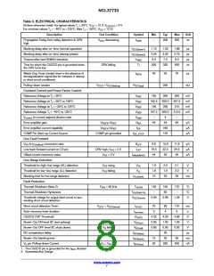
NCL37733
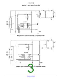
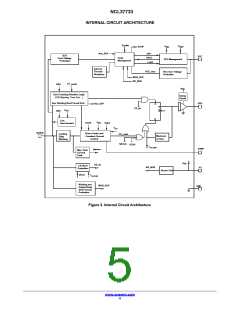
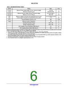
Table 1. PIN FUNCTION DESCRIPTION
Pin #
Pin Name
Function
Pin Description
1
CS/ZCD
Current Sense and Zero This multi−function pin is designed to monitor the primary peak current for protection
Current Detection
and output current control and the auxiliary winding voltage for zero current detection
2
3
GND
Controller ground pin
COMP
Filtering Capacitor
This pin receives a filtering capacitor for power factor correction. Typical values
ranges from 0.47 − 4.70 mF
4
V
S
Input Voltage Sensing
This pin observes the input voltage rail and protects the LED driver in case of too low
mains conditions (brown−out). This pin also observes the input voltage rail for:
− Power Factor Correction
− Line Range Detection
5
6
V
IC Supply Pin
Driver Output
This pin is the positive supply of the IC. The circuit starts to operate when V
CC
CC
exceeds 18 V and turns off when V goes below 8.8 V (typical values). After
CC
start−up, the operating range is 9.4 V up to 25.5 V (V
minimum level).
CC(OVP)
DRV
The driver’s output to an external MOSFET
www.onsemi.com
3

 ONSEMI [ ONSEMI ]