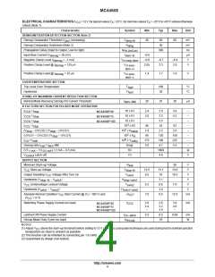
MC44608
• 2. Overload
according to the equation of the current sense section, page
5. The C.S. clamping level depends on the power to be
delivered to the load during the SMPS stand–by mode.
Every switching sequence ON/OFF is terminated by an OC
as long as the secondary Zener diode voltage has not been
reached. When the Zener voltage is reached the ON cycle is
terminated by a true PWM action. The proper SWITCHING
PHASE termination must correspond to a NOC condition.
The LW latch stores this NOC status.
The LATCHED OFF PHASE: The MODE latch is set.
The START–UP PHASE is similar to the Overload Mode.
The MODE latch remains in its set status (Q=1).
The SWITCHING PHASE: The Stand–by signal is
validated and the 200µA is sourced out of the Current Sense
pin 2.
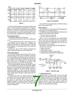
In the hiccup mode the 3 distinct phases are described as
follows (refer to Figure 6):
The SWITCHING PHASE: The SMPS output is low and
the regulation block reacts by increasing the ON time (dmax
= 80%). The OC is reached at the end of every switching
cycle. The LW latch (Figure 7) is reset before the VPWM
signal appears. The SMPS output voltage is low. The V
CC
voltage cannot be maintained at a normal level as the
auxiliary winding provides a voltage which is also reduced
in a ratio similar to the one on the output (i.e. Vout nominal
/ Vout short–circuit). Consequently the V
CC
reduced at an operating rate given by the combination V
voltage is
CC
capacitor value together with the I working consumption
CC
(3.2mA) according to the equation 2. When V
crosses
CC
10V the WORKING PHASE gets terminated. The LW latch
remains in the reset status.
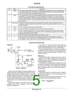
• 4. Transition from Stand–by to Normal
The secondary reconfiguration is removed. The
regulation on the low voltage secondary rail can no longer
be achieved, thus at the end of the SWITCHING PHASE, no
PWM condition can be encountered. The LW latch is reset.
At the next WORKING PHASE a NORMAL mode status
takes place.
In order to become independent of the recovery time
constant on the secondary side of the SMPS an additional
resetinputR2isprovidedontheMODElatch. Thecondition
Idemag<24µA corresponds to the activation of the
secondary reconfiguration status. The R2 reset insures a
return into the NORMAL mode following the first
START–UP PHASE.
The LATCHED–OFF PHASE: The V
capacitor
CC
voltage continues to drop. When it reaches 6.5V this phase
is terminated. Its duration is governed by equation 3.
The START–UP PHASE is reinitiated. The high voltage
start–up current source (–I
MODE latch is reset. The V
= 9mA) is activated and the
voltage ramps up according
CC1
CC
to the equation 1. When it reaches 13V, the IC enters into the
SWITCHING PHASE.
The NEXT SWITCHING PHASE: The high voltage
current source is inhibited, the MODE latch (Q=0) activates
the NORMAL mode of operation. Figure 2 shows that no
current is injected out pin 2. The over current sense level
corresponds to 1V.
As long as the overload is present, this sequence repeats.
TheSWITCHINGPHASEdutycycleisintherangeof10%.
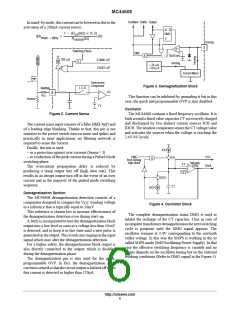
Pulsed Mode Duty Cycle Control
During the sleep mode of the SMPS the switch S3 is
closed and the control input pin 3 is connected to a 4.6V
voltagesource thrua 500 resistor. Thedischargerateofthe
• 3. Transition from Normal to Pulsed Mode
In this sequence the secondary side is reconfigured (refer
to the typical application schematic on page 13). The high
voltage output value becomes lower than the NORMAL
mode regulated value. The TL431 shunt regulator is fully
OFF. In the SMPS stand–by mode all the SMPS outputs are
lowered except for the low voltage output that supply the
wake–up circuit located at the isolated side of the power
supply. In that mode the secondary regulation is performed
by the zener diode connected in parallel to the TL431.
The secondary reconfiguration status can be detected on
the SMPS primary side by measuring the voltage level
present on the auxiliary winding Laux. (Refer to the
Demagnetization Section). In the reconfigured status, the
V
CC
capacitor is given by I (device consumption
CC–latch
during the LATCHED OFF phase) in addition to the current
drawn out of the pin 3. Connecting a resistor between the Pin
3 and GND (R
) a programmable current isdrawn
DPULSED
from the V through pin 3. The duration of the LATCHED
CC
OFF phase is impacted by the presence of the resistor
R
. The equation 3 shows the relation to the pin 3
DPULSED
current.
Pulsed Mode Phases
Equations 1 through 8 define and predict the effective
behavior during the PULSED MODE operation. The
equations 6, 7, and 8 contain K, Y, and D factors. These
factors are combinations of measured parameters. They
appear in the parameter section “Kfactors for pulsed mode
operation” page 4. In equations 3 through 8 the pin 3 current
is the current defined in the above section “Pulsed Mode
Duty Cycle Control”.
Laux voltage is also reduced. The V
self–powering is no
CC
longer possible thus the SMPS enters in a hiccup mode
similar to the one described under the Overload condition.
In the SMPS stand–by mode the 3 distinct phases are:
The SWITCHING PHASE: Similar to the Overload
mode. The current sense clamping level is reduced
http://onsemi.com
8

 ONSEMI [ ONSEMI ]