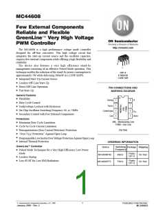
MC44608
PIN FUNCTION DESCRIPTION
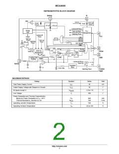
Description
Pin
Name
1
Demag
The Demag pin offers 3 different functions: Zero voltage crossing detection (50mV), 24µA current detection
and 120µA current detection. The 24µA level is used to detect the secondary reconfiguration status and the
120µA level to detect an Over Voltage status called Quick OVP.
2
I
The Current Sense pin senses the voltage developed on the series resistor inserted in the source of the
sense
power MOSFET. When I
reaches 1V, the Driver output (pin 5) is disabled. This is known as the Over
sense
Current Protection function. A 200µA current source is flowing out of the pin 3 during the start–up phase and
during the switching phase in case of the Pulsed Mode of operation. A resistor can be inserted between the
sense resistor and the pin 3, thus a programmable peak current detection can be performed during the SMPS
stand–by mode.
3
Control Input
A feedback current from the secondary side of the SMPS via the opto–coupler is injected into this pin. A
resistor can be connected between this pin and GND to allow the programming of the Burst duty cycle during
the Stand–by mode.
4
5
6
Ground
Driver
This pin is the ground of the primary side of the SMPS.
The current and slew rate capability of this pin are suited to drive Power MOSFETs.
V
CC
This pin is the positive supply of the IC. The driver output gets disabled when the voltage becomes higher
than 15V and the operating range is between 6.6V and 13V. An intermediate voltage level of 10V creates a
disabling condition called Latched Off phase.
7
8
This pin is to provide isolation between the Vi pin 8 and the V pin 6.
CC
Vi
This pin can be directly connected to a 500V voltage source for start–up function of the IC. During the
Start–up phase a 9 mA current source is internally delivered to the V pin 6 allowing a rapid charge of the
CC
capacitor. As soon as the IC starts–up, this current source is disabled.
V
CC
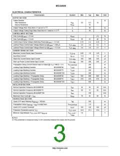
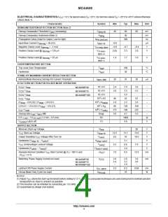
OPERATING DESCRIPTION
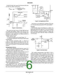
The switch S3 is closed in Stand–by mode during the
Regulation
Latched Off Phase while the switch S2 remains open. (See
section PULSED MODE DUTY CYCLE CONTROL).
The resistor Rdpulsed (Rduty cycle burst) has no effect on
the regulation process. This resistor is used to determine the
burstdutycycledescribedinthechapter“PulsedDutyCycle
Control” on page 8.
V
LP–stby
V
CC
1
0
Stand–by
Latched off Phase
Control
Input
&
S3
3
1
0
Switching Phase
PWM
PWM Latch
S2
V
dd
The MC44608 works in voltage mode. The on–time is
controlled by the PWM comparator that compares the
oscillator sawtooth with the regulation block output (refer to
the block diagram on page 2).
The PWM latch is initialized by the oscillator and is reset
by the PWM comparator or by the current sense comparator
in case of an over current. This configuration ensures that
only a single pulse appears at the circuit output during an
oscillator cycle.
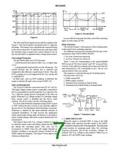
Regulation
Output
20
Comparator
5 V
4 kHz
Filter
1.6 V
Figure 1. Regulator
Current Sense
The inductor current is converted to a positive voltage by
inserting a ground reference sense resistor R
with the power switch.
The maximum current sense threshold is fixed at 1V. The
peak current is given by the following equation:
Thepin3sensesthefeedbackcurrentprovidedbytheopto
coupler. During the switching phase the switch S2 is closed
and the shunt regulator is accessible by the pin 3. The shunt
regulator voltage is typically 5V. The dynamic resistance of
the shunt regulator represented by the zener diode is 20 .
The gain of the Control input is given on Figure 10 which
showsthedutycycleasafunctionofthecurrentinjectedinto
the pin 3.
in series
Sense
1
Ipk
(A)
max
R
( )
sense
A 4kHz filter network is inserted between the shunt
regulator and the PWM comparator to cancel the high
frequency residual noise.
http://onsemi.com
5

 ONSEMI [ ONSEMI ]