MC44608
OSC
4 V
V
CC
13 V
Vcont
2.4 V
10 V
Clock
6.5 V
DMG
Iprim
Start–up
Phase
Latched off
Phase
Switching
Phase
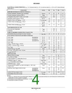
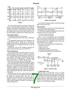
Figure 6. Hiccup Mode
Figure 5.
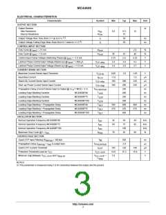
In case of the hiccup mode, the duty cycle of the switching
phase is in the range of 10%.
The OSC and Clock signals are provided according to the
Figure 5. The Clock signals correspond to the CT capacitor
discharge. The bottom curve represents the current flowing
in the sense resistor Rcs. It starts from zero and stops when
the sawtooth value is equal to the control voltage Vcont. In
this way the SMPS is regulated with a voltage mode control.
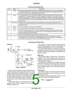
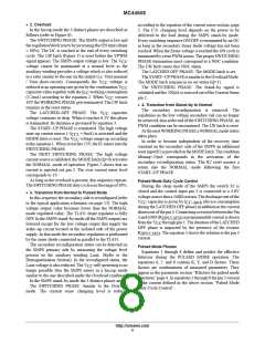
Mode Transition
TheLWlatchFigure7isthememoryoftheworkingstatus
at the end of every switching sequence.
Two different cases must be considered for the logic at the
termination of the SWITCHING PHASE:
1. No Over Current was observed
2. An Over Current was observed
Overvoltage Protection
The MC44608 offers two OVP functions:
These 2 cases are corresponding to the signal labelled
NOCincaseof“NoOverCurrent”and“OC”incaseofOver
Current. So the effective working status at the end of the ON
time memorized in LW corresponds to Q=1 for no over
current and Q=0 for over current.
– a fixed function that detects when V
15.4V
is higher than
CC
– a programmable function that uses the demag pin. The
current flowing into the demag pin is mirrored and
compared to the reference current Iovp (120µA). Thus this
OVP is quicker as it is not impacted by the V
is called QOVP.
This sequence is repeated during the Switching phase.
Several events can occur:
inertia and
CC
1. SMPS switch OFF
2. SMPS output overload
3. Transition from Normal to Pulsed Mode
4. Transition from Pulsed Mode to Normal Mode
In both cases, once an OVP condition is detected, the
output is latched off until a new circuit START–UP.
Start–up Management
The Vi pin 8 is directly connected to the HV DC rail Vin.
This high voltage current source is internally connected to
Latched Off
Phase
theV pinandthusisusedtochargetheV capacitor.The
CC CC
V
capacitor charge period corresponds to the Start–up
CC
VPWM
OUT
NOC
OC
S
Q
Q
Stand–by
&
&
S
Mode
&
&
phase. When the V voltage reaches 13V, the high voltage
CC
Q
LW
9mA current source is disabled and the device starts
working. The device enters into the switching phase.
It is to be noticed that the maximum rating of the Vi pin 8
is 700V. ESD protection circuitry is not currently added to
this pin due to size limitations and technology constraints.
Protection is limited by the drain–substrate junction in
avalanche breakdown. To help increase the application
safety against high voltage spike on that pin it is possible to
insert a small wattage 1k series resistor between the Vin
rail and pin 8.
S1
R1
R2
R
Switch
LEB out
1 V
+
CS
–
I
Start–up
Phase > 24
Switching Start–up
Phase Phase
demag
A
Figure 7. Transition Logic
• 1. SMPS SWITCH OFF
When the mains is switched OFF, so long as the bulk
electrolithic bulk capacitor provides energy to the SMPS,
the controller remains in the switching phase. Then the peak
current reaches its maximum peak value, the switching
frequency decreases and all the secondary voltages are
The Figure 6 shows the V
no external current source providing current into the V
voltage evolution in case of
CC
CC
pin during the switching phase. This case can be
encountered in SMPS when the self supply through an
auxiliary winding is not present (strong overload on the
SMPS output for example). The Figure 16 also depicts this
working configuration.
reduced. The V
voltage is also reduced. When V is
CC
equal to 10V, the SMPS stops working.
CC
http://onsemi.com
7

 ONSEMI [ ONSEMI ]