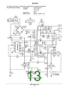
MC44608
60
50
5.08
5.07
5.06
5.05
t_rise
85° C
5.04
5.03
40
30
20
10
t_fall
25° C
5.02
5.01
–25° C
5.00
4.99
4.98
0.5
1
1.5
Current Injected in Pin 3 (mA)
2
2.5
10
11
12
13
14
15
Pin6 V Voltage (V)
CC
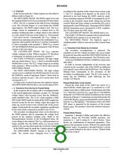
Figure 8. Output Switching Speed
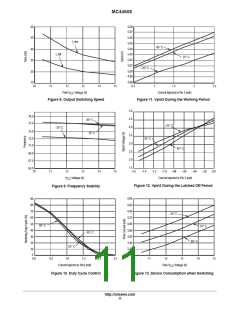
Figure 11. Vpin3 During the Working Period
5.0
4.5
4.0
3.5
3.0
2.5
2.0
1.5
79.0
77.0
85° C
–25° C
–25° C
75.0
25° C
25° C
73.0
71.0
85° C
69.0
67.0
65.0
10
11
12
13
14
15
–1.6
–1.4
–1.2
–1.0 –.08
–.06
–.04
–.02
0.0
V
CC
Voltage (V)
Current Injected in Pin 3 (mA)
Figure 12. Vpin3 During the Latched Off Period
Figure 9. Frequency Stability
4.80
4.60
4.40
4.20
4.00
90
80
70
60
50
40
–25° C
85° C
25° C
3.80
3.60
3.40
3.20
3.00
–25° C
30
20
10
0
85° C
25° C
0.0
0.5
1.0
1.5
2.0
2.5
10
11
12
13
14
15
Current Injected in Pin3 (mA)
Pin6 V Voltage (V)
CC
Figure 10. Duty Cycle Control
Figure 13. Device Consumption when Switching
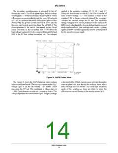
http://onsemi.com
11

 ONSEMI [ ONSEMI ]