MC44608
Oscillator Buffer Output
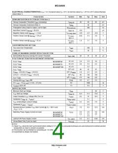
Instand–bymode, thiscurrentcanbeloweredasduetothe
activation of a 200µA current source:
R Q
DMG
1
(R (k ) 0, 2)
cs
Ipk
(A)
max stby
R
( )
S
sense
Demag
1
+
–
Switching Phase
&
DMG
&
50/20 mV
200
0
A
STAND–BY
START–UP
Idemag
> 24
>120
A
A
1
Current Mirror
Overcurrent
Comparator
Figure 3. Demagnetization Block
L.E.B.
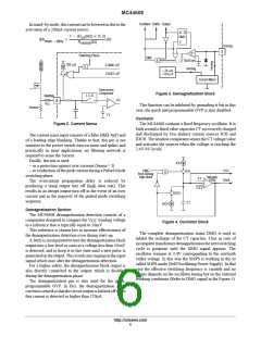
Isense
OC
+
–
2
Rcs
This function can be inhibited by grounding it but in this
case, the quick and programmable OVP is also disabled.
Rsense
1 V
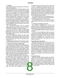
Oscillator
Figure 2. Current Sense
The MC44608 contains a fixed frequency oscillator. It is
built around a fixed value capacitor CT succesively charged
and discharged by two distinct current sources ICH and
IDCH. The window comparator senses the CT voltage value
and activates the sources when the voltage is reaching the
2.4V/4V levels.
The current sense input consists of a filter (6k , 4pF) and
of a leading edge blanking. Thanks to that, this pin is not
sensitive to the power switch turn on noise and spikes and
practically in most applications, no filtering network is
required to sense the current.
Finally, this pin is used:
ICH
– as a protection against over currents (Isense > I)
– as a reduction of the peak current during a Pulsed Mode
switching phase.
DMG
from Demag
logic block
OSC
SCH
&
Window
comp
4 V
+
–
Clock
The overcurrent propagation delay is reduced by
producing a sharp output turn off (high slew rate). This
results in an abrupt output turn off in the event of an over
current and in the majority of the pulsed mode switching
sequense.
2.4 V
SDCH
CT
IDCH
Demagnetization Section
The MC44608 demagnetization detection consists of a
comparator designed to compare the V
to a reference that is typically equal to 50mV.
winding voltage
CC
Figure 4. Oscillator Block
This reference is chosen low to increase effectiveness of
the demagnetization detection even during start–up.
A latch is incorporated to turn the demagnetization block
output into a low level as soon as a voltage less than 50 mV
is detected, and to keep it in this state until a new pulse is
generatedon the output. This avoids any ringing on the input
signal which may alter the demagnetization detection.
For a higher safety, the demagnetization block output is
also directly connected to the output, which is disabled
during the demagnetization phase.
The complete demagnetization status DMG is used to
inhibit the recharge of the CT capacitor. Thus in case of
incomplete transformer demagnetization the next switching
cycle is postpone until the DMG signal appears. The
oscillator remains at 2.4V corresponding to the sawtooth
valley voltage. In this way the SMPS is working in the so
called SOPS mode (Self Oscillating Power Supply). In that
case the effective switching frequency is variable and no
longer depends on the oscillator timing but on the external
working conditions (Refer to DMG signal in the Figure 5).
The demagnetization pin is also used for the quick,
programmable OVP. In fact, the demagnetization input
current is sensed so that the circuit output is latched offwhen
this current is detected as higher than 120µA.
http://onsemi.com
6

 ONSEMI [ ONSEMI ]