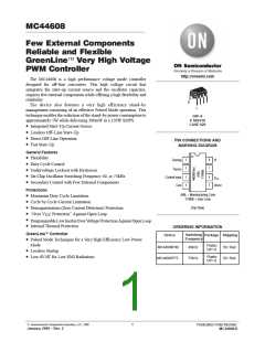
MC44608
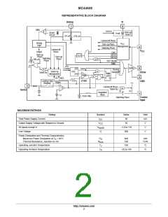
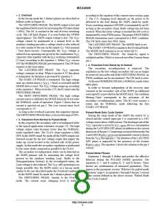
REPRESENTATIVE BLOCK DIAGRAM
Demag
Vi
1
8
DMG
+
–
UVLO2
Start–up
Source
50 mV
/20 mV
9 mA
>24
A
>120
A
Latched off Phase
Start–up Phase
Switching Phase
Demag
Logic
V
CC
Management
6
Latched off
Phase
V
CC
Output
Start–up
Phase
OVP
UVLO1
UVLO2
2 S
Start–up
Phase
Switching
Phase
&
200
0
A
OUT Disable
DMG
1
OSC
Enable
S1
Buffer
5
4
Clock
&
Thermal
Shutdown
&
S
Stand–by
Management
OSC
Driver
GND
Stand–by
+
PWM
Latch
PWM
–
&
R
OC NOC
Output
Q
&
Leading Edge
Blanking
VPWM
+
2
Latched off Phase
Stand–by
CS
&
Isense
–
S2
S3
Regulation
3
Block
1 V
4 kHz Filter
Switching Phase
Control
Input
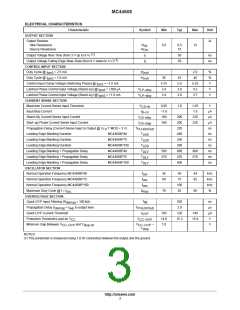
MAXIMUM RATINGS
Rating
Symbol
Value
30
Unit
mA
V
Total Power Supply Current
I
CC
Output Supply Voltage with Respect to Ground
All Inputs except Vi
V
CC
16
V
inputs
–1.0 to +16
500
V
Line Voltage
V
i
V
Power Dissipation and Thermal Characteristics
Maximum Power Dissipation at T = 85°C
Thermal Resistance, Junction–to–Air
P
600
100
mW
°C/W
A
D
R
θJA
Operating Junction Temperature
T
150
°C
°C
J
Operating Ambient Temperature
T
A
–25 to +85
http://onsemi.com
2

 ONSEMI [ ONSEMI ]