TJA1028
NXP Semiconductors
LIN transceiver with integrated voltage regulator
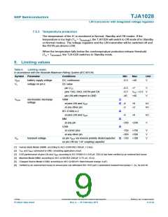
7.5.3 Temperature protection
The temperature of the IC is monitored in Normal, Standby and Off modes. If the
temperature is too high (Tvj > Tth(act)otp), the TJA1028 will switch to Off mode (if in Standby
or Normal modes). The voltage regulator and the LIN transmitter will be switched off and
the RSTN pin driven LOW.
When the temperature falls below the overtemperature protection release threshold
(Tvj < Tth(rel)otp), the TJA1028 switches to Standby mode.
8. Limiting values
Table 4.
Limiting values
In accordance with the Absolute Maximum Rating System (IEC 60134).
Symbol Parameter
Conditions
Min
Max
Unit
VBAT
Vx
battery supply voltage
DC; continuous
−0.3
+40
V
voltage on pin x
DC value
pin VCC
−0.3
−0.3
−40
+7
V
V
V
pins TXD, RXD, RSTN and EN
VCC + 0.3
+40
pin LIN with respect to GND
[1]
[2]
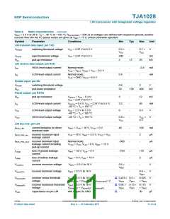
VESD
electrostatic discharge
voltage
HBM
at pins LIN and VBAT
−8
−2
+8
+2
kV
kV
at any other pin
[3]
[4]
[5]
IEC 61000-4-2
at pins LIN and VBAT
−8
+8
kV
V
MM
at any pin
−250 +250
CDM
at corner pins
−750 +750
−500 +500
−150 +100
V
V
V
at any other pin
[6]
Vtrt
transient voltage
on pin VBAT via reverse polarity diode/capacitor;
on pin LIN via 1 nF coupling capacitor
[1] Human Body Model (HBM): according to AEC-Q100-002 (100 pF, 1.5 kΩ).
[2] VCC and VBAT connected to GND, emulating application circuit.
[3] ESD performance of pins LIN and VBAT according to IEC 61000-4-2 (150 pF, 330 Ω) has been verified by an external test house.
[4] Machine Model (MM): according to AEC-Q100-003 (200 pF, 0.75 μH, 10 Ω).
[5] Charged Device Model (CDM): according to AEC-Q100-011 (field Induced charge; 4 pF).
[6] Verified by an external test house to ensure pins can withstand ISO 7637 part 2 automotive transient test pulses 1, 2a, 3a and 3b.
TJA1028
All information provided in this document is subject to legal disclaimers.
© NXP B.V. 2011. All rights reserved.
Product data sheet
Rev. 2 — 25 February 2011
9 of 24

 NXP [ NXP ]