TJA1028
NXP Semiconductors
LIN transceiver with integrated voltage regulator
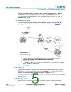
The TJA1028 switches from Off mode to Standby mode as soon as the battery supply
voltage rises above the power-on detection threshold (VBAT > Vth(det)pon), provided the
junction temperature is below the overtemperature protection release threshold
(Tvj < Tth(rel)otp).
The TJA1028 switches to Standby mode from Normal mode during the mode select
window if TXD is HIGH and EN is LOW (see Section 7.1.5), provided RSTN = 1.
A remote wake-up event will trigger a transition to Standby mode from Sleep mode. The
remote wake-up event will be signalled by a continuous LOW level on pin RXD.
In Standby mode, the voltage regulator is on, the LIN physical layer is disabled and
remote wake-up detection is active. The wake-up source is indicated by the level on RXD
(LOW indicates a remote wake-up).
7.1.3 Normal mode
If the EN pin is pulled HIGH while the TJA1028 is in Standby mode (with RSTN = 1) or
Sleep mode, the device will enter Normal mode. The LIN physical layer and the voltage
regulator are enabled in Normal mode.
7.1.3.1 The LIN transceiver in Normal mode
The LIN transceiver is activated when the TJA1028 enters Normal mode.
In Normal mode, the transceiver can transmit and receive data via the LIN bus. The
receiver detects data streams on the LIN pin and transfers them to the microcontroller via
pin RXD. LIN recessive is represented by a HIGH level on RXD, LIN dominant by a LOW
level.
The transmit data streams of the protocol controller at the TXD input are converted by the
transmitter into bus signals with optimized slew rate and wave shaping to minimize EME.
A LOW level at the TXD input is converted to a LIN dominant level while a HIGH level is
converted to a LIN recessive level.
7.1.4 Sleep mode
Sleep mode features extremely low power consumption.
The TJA1028 switches to Sleep mode from Normal mode during the mode select window
if TXD and EN are both LOW (see Section 7.1.5), provided RSTN = 1.
The voltage regulator and the LIN physical layer are disabled in Sleep mode. Pin RSTN is
forced LOW. Remote wake-up detection is active.
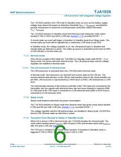
7.1.5 Transition from Normal to Sleep or Standby mode
When EN is driven LOW in Normal mode, the TJA1028 disables the transmit path. The
mode select window opens tmsel(min) after EN goes LOW, and remains open until tmsel(max)
after EN goes LOW (see Figure 4).
The TXD pin is sampled in the mode select window. A transition to Standby mode is
triggered if TXD is HIGH, or to Sleep mode if TXD is LOW.
TJA1028
All information provided in this document is subject to legal disclaimers.
© NXP B.V. 2011. All rights reserved.
Product data sheet
Rev. 2 — 25 February 2011
6 of 24

 NXP [ NXP ]