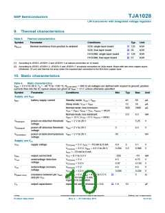
TJA1028
NXP Semiconductors
LIN transceiver with integrated voltage regulator
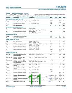
Table 6.
Static characteristics …continued
VBAT = 5.5 V to 28 V; Tvj = −40 °C to +150 °C; RL(LIN-VBAT) = 500 Ω; all voltages are defined with respect to ground; positive
currents flow into the IC; typical values are given at VBAT = 12 V; unless otherwise specified.
Symbol
Parameter
Conditions
Min
Typ
Max
Unit
LIN transmit data input; pin TXD
Vth(sw)
switching threshold voltage
VCC = 2.97 V to 5.5 V
VCC = 2.97 V to 5.5 V
0.3 ×
VCC
-
0.7 ×
VCC
V
Vhys(i)
Rpu
input hysteresis voltage
pull-up resistance
200
5
-
-
mV
12
25
kΩ
LIN receive data output; pin RXD
IOH
HIGH-level output current
Normal mode;
VLIN = VBAT; VRXD = VCC − 0.4 V
-
-
-
−0.4
mA
mA
IOL
LOW-level output current
Normal mode;
0.4
-
VLIN = GND; VRXD = 0.4 V
Enable input; pin EN
Vth(sw)
Rpd
switching threshold voltage
pull-down resistance
0.8
50
-
2
V
130
400
kΩ
Reset output; pin RSTN
Rpu pull-up resistance
VRSTN = VCC − 0.4 V;
VCC = 2.97 V to 5.5 V
3
-
-
-
-
12
40
0.5
kΩ
mA
V
IOL
LOW-level output current
LOW-level output voltage
HIGH-level output voltage
VRSTN = 0.4 V; VCC = 2.97 V to 5.5 V;
−40 °C < Tvj < 195 °C
3.2
0
VOL
VOH
VCC = 2.5 V to 5.5 V;
−40 °C < Tvj < 195 °C
−40 °C < Tvj < 195 °C
0.8 ×
VCC
VCC
0.3
+
V
LIN bus line; pin LIN
IBUS_LIM
current limitation for driver
dominant state
VBAT = VLIN = 18 V; VTXD = 0 V
40
-
-
-
-
100
mA
μA
μA
IBUS_PAS_rec
receiver recessive input
leakage current
VLIN = 18 V; VBAT = 5.5 V; VTXD = VCC
2
-
IBUS_PAS_dom receiver dominant input
leakage current including
pull-up resistor
Normal mode;
VTXD = VCC; VLIN = 0 V; VBAT = 12 V
−600
IL(log)
loss of ground leakage
current
VBAT = 18 V; VLIN = 0 V
VBAT = 0 V; VLIN = 18 V
VBAT = 5.5 V to 18 V
VBAT = 5.5 V to 18 V
−750
-
-
-
-
+10
μA
μA
V
IL(lob)
loss of battery leakage
current
-
2
-
Vrec(RX)
Vdom(RX)
Vth(cntr)RX
Vth(hys)RX
CLIN
receiver recessive voltage
0.6 ×
VBAT
receiver dominant voltage
-
0.4 ×
VBAT
V
[2]
[2]
[1]
receiver center threshold
voltage
VBAT = 5.5 V to 18 V;
Vth(cntr)RX = (Vth(rec)RX + Vth(dom)RX) / 2
0.475 × 0.5 ×
VBAT VBAT
0.525
× VBAT
V
receiver hysteresis threshold VBAT = 5.5 V to 18 V;
voltage
0.05 × 0.15 × 0.175
VBAT
V
Vth(hys)RX = Vth(rec)RX - Vth(dom)RX
VBAT
× VBAT
capacitance on pin LIN
with respect to GND
-
-
30
pF
TJA1028
All information provided in this document is subject to legal disclaimers.
© NXP B.V. 2011. All rights reserved.
Product data sheet
Rev. 2 — 25 February 2011
11 of 24

 NXP [ NXP ]