TJA1028
NXP Semiconductors
LIN transceiver with integrated voltage regulator
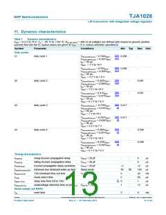
11. Dynamic characteristics
Table 7.
BAT = 5.5 V to 18 V; Tvj = −40 °C to +150 °C; RL(LIN-VBAT) = 500 Ω; all voltages are defined with respect to ground; positive
currents flow into the IC; typical values are given at VBAT = 12 V; unless otherwise specified.[1]
Dynamic characteristics
V
Symbol
Duty cycles
δ1
Parameter
Conditions
Min Typ
Max Unit
[2][3]
[4][5]
duty cycle 1
Vth(rec)RX(max) = 0.744VBAT
;
0.396 -
-
Vth(dom)RX(max) = 0.581VBAT
bit = 50 μs;
VBAT = 7 V to 18 V
;
;
t
[2][3]
[4][5]
Vth(rec)RX(max) = 0.76VBAT
;
0.396 -
-
Vth(dom)RX(max) = 0.593VBAT
t
bit = 50 μs;
VBAT = 5.5 V to 7.0 V
[2][4]
[5][6]
δ2
δ3
δ4
duty cycle 2
duty cycle 3
duty cycle 4
V
th(rec)RX(min) = 0.422VBAT
;
-
-
-
-
0.581
0.581
-
Vth(domRX)(min) = 0.284VBAT;
tbit = 50 μs;
VBAT = 7.6 V to 18 V
[2][4]
[5][6]
V
th(rec)RX(min) = 0.41VBAT;
Vth(dom)RX(min) = 0.275VBAT
tbit = 50 μs;
VBAT = 6.1 V to 7.6 V
;
[3][4]
[5]
V
th(rec)RX(max) = 0.778VBAT
;
0.417 -
0.417 -
Vth(dom)RX(max) = 0.616VBAT
tbit = 96 μs;
VBAT = 7 V to 18 V
;
;
[3][4]
[5]
V
th(rec)RX(max) = 0.797VBAT
;
-
Vth(dom)RX(max) = 0.630VBAT
tbit = 96 μs;
VBAT = 5.5 V to 7 V
[4][5]
[6]
V
th(rec)RX(min) = 0.389VBAT
-
-
-
-
0.590
0.590
Vth(dom)RX(min) = 0.251VBAT
tbit = 96 μs
VBAT = 7.6 V to 18 V
[4][5]
[6]
V
V
th(rec)RX(min) = 0.378VBAT
th(dom)RX(min) = 0.242VBAT
;
;
tbit = 96 μs;
VBAT = 6.1 V to 7.6 V
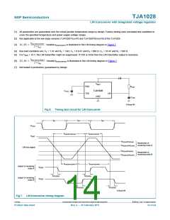
Timing characteristics
tPD(RX)r
rising receiver propagation delay
CRXD = 20 pF
CRXD = 20 pF
CRXD = 20 pF
Sleep mode
VTXD = 0 V
-
-
6
μs
μs
μs
μs
ms
μs
μs
μs
tPD(RX)f
falling receiver propagation delay
-
-
6
tPD(RX)sym
receiver propagation delay symmetry
−2
30
6
-
+2
150
20
20
1
twake(busdom)min minimum bus dominant wake-up time
80
-
tto(dom)TXD
tmsel
td(EN-TXD)
tdet(uv)(VCC)
Reset output; pin RSTN
TXD dominant time-out time
mode select time
3
-
[7]
delay time from EN to TXD
0
-
undervoltage detection time on pin VCC CRSTN = 20 pF
1
-
15
trst
reset time
2
-
8
ms
TJA1028
All information provided in this document is subject to legal disclaimers.
© NXP B.V. 2011. All rights reserved.
Product data sheet
Rev. 2 — 25 February 2011
13 of 24

 NXP [ NXP ]