TJA1028
NXP Semiconductors
LIN transceiver with integrated voltage regulator
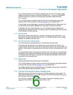
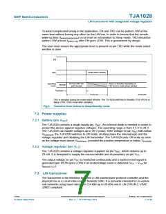
To avoid complicated timing in the application, EN and TXD can be pulled LOW at the
same time without having any effect on the LIN bus. In order to ensure that the remote
wake-up time (twake(busdom)min) is not reset on a transition to Sleep mode, TXD should be
pulled LOW at least td(EN-TXD) after EN goes LOW. This is guaranteed by design.
The user must ensure the appropriate level is present on pin TXD while the mode select
window is open.
EN
TXD
mode select window
operating
mode
Normal withTXD
path blocked
Sleep or Standby depending on
TXD level in mode select window
Normal
t
msel(min)
t
msel(max)
015aaa087
TXD is sampled during the mode select window. The TJA1028 switches to Standby (TXD HIGH) or
Sleep (TXD LOW) mode after sampling.
Fig 4. Transition from Normal to Sleep/Standby mode
7.2 Power supplies
7.2.1 Battery (pin VBAT
)
The TJA1028 contains a single supply pin, VBAT. An external diode is needed in series to
protect the device against negative voltages. The operating range is from 4.5 V to 28 V.
The TJA1028 can handle voltages up to 40 V (max). If the voltage on pin VBAT falls below
V
th(det)poff, the TJA1028 switches to Off mode, shutting down the internal logic and the
voltage regulator and disabling the LIN transmitter. The TJA1028 exits Off mode as soon
as the voltage rises above Vth(det)pon, provided the junction temperature is below Tth(rel)otp
.
7.2.2 Voltage regulator (pin VCC
)
The TJA1028 contains a voltage regulator supplied via pin VBAT, which delivers up to
70 mA. It is designed to supply the microcontroller and its periphery via pin VCC
.
The output voltage on pin VCC is monitored continuously and a system reset signal is
generated (pin RSTN goes LOW) if an undervoltage event is detected (VCC < Vuvd for
tdet(uv)(VCC)).
7.3 LIN transceiver
The transceiver is the interface between a LIN master/slave protocol controller and the
physical bus in a Local Interconnect Network (LIN). It is primarily intended for in-vehicle
sub-networks using baud rates from 2.4 kBd up to 20 kBd and is LIN 2.0/LIN 2.1/SAE
J2602 compliant.
TJA1028
All information provided in this document is subject to legal disclaimers.
© NXP B.V. 2011. All rights reserved.
Product data sheet
Rev. 2 — 25 February 2011
7 of 24

 NXP [ NXP ]