TJA1028
NXP Semiconductors
LIN transceiver with integrated voltage regulator
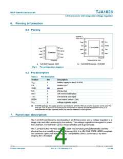
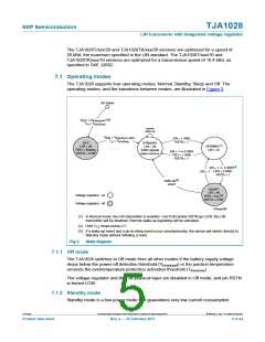
6. Pinning information
6.1 Pinning
terminal 1
index area
1
2
3
4
8
7
6
5
V
V
CC
BAT
EN
RSTN
TXD
TJA1028TK
1
2
3
4
8
7
6
5
V
V
CC
BAT
GND
LIN
RSTN
TXD
EN
TJA1028T
RXD
GND
LIN
RXD
015aaa244
Transparent top view
015aaa082
a. TJA1028T/xxx/xx: SO8
Fig 2. Pin configuration diagrams
b. TJA1028TK/xxx/xx: HVSON8
6.2 Pin description
Table 3.
Pin description
Symbol
VBAT
EN
Pin
1
Description
battery supply for the TJA1028
enable input
2
GND
LIN
3[1]
ground
4
LIN bus line
RXD
TXD
RSTN
VCC
5
LIN receive data output
LIN transmit data input
reset output (active LOW)
voltage regulator output
6
7
8
[1] HVSON8 package die supply ground is connected to both the GND pin and the exposed center pad. The
GND pin must be soldered to board ground. For enhanced thermal and electrical performance, it is
recommended that the exposed center pad also be soldered to board ground.
7. Functional description
The TJA1028 combines the functionality of a LIN transceiver and a voltage regulator in a
single chip and offers wake-up by bus activity. The voltage regulator is designed to power
the Electronic Control Unit’s (ECU) microcontroller and its peripherals.
The TJA1028 is the interface between a LIN master/slave protocol controller and the
physical bus in a Local Interconnect Network (LIN). It is LIN 2.0/2.1/SAE J2602 compliant
and achieves optimum ElectroMagnetic Compatibility (EMC) performance by wave
shaping the LIN output.
TJA1028
All information provided in this document is subject to legal disclaimers.
© NXP B.V. 2011. All rights reserved.
Product data sheet
Rev. 2 — 25 February 2011
4 of 24

 NXP [ NXP ]