TJA1028
NXP Semiconductors
LIN transceiver with integrated voltage regulator
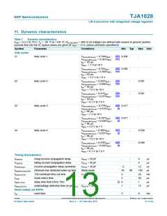
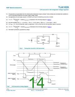
[1] All parameters are guaranteed over the virtual junction temperature range by design. Factory testing uses correlated test conditions to
cover the specified temperature and power supply voltage ranges.
[2] Not applicable to the low slope versions (TJA1028T/xxx/10 and TJA1028TK/xxx/10) of the TJA1028.
tbus(rec)(min)
[3] δ1, δ3 =
. Variable tbus(rec)(min) is illustrated in the LIN timing diagram in Figure 7.
-------------------------------
2 × tbit
[4] Bus load conditions are: CL = 1 nF and RL = 1 kΩ; CL = 6.8 nF and RL = 660 Ω; CL = 10 nF and RL = 500 Ω.
[5] For VBAT > 18 V, the LIN transmitter might be suppressed. If TXD is HIGH then the LIN transmitter output is recessive.
tbus(rec)(max)
[6] δ2, δ4 =
. Variable tbus(rec)(max) is illustrated in the LIN timing diagram in Figure 7.
-------------------------------
2 × tbit
[7] Not tested in production; guaranteed by design.
V
BAT
RXD
TXD
R
LIN
TJA1028
C
RXD
LIN
GND
C
LIN
015aaa198
Fig 6. Timing test circuit for LIN transceiver
t
t
t
bit
bit
bit
V
TXD
t
t
bus(rec)(min)
bus(dom)(max)
V
BAT
V
V
th(rec)RX(max)
thresholds of
receiving node A
th(dom)RX(max)
LIN bus signal
V
V
th(rec)RX(min)
thresholds of
receiving node B
th(dom)RX(min)
t
t
bus(rec)(max)
bus(dom)(min)
output of receiving
node A
V
V
RXD
t
t
PD(RX)r
PD(RX)f
output of receiving
node B
RXD
t
t
PD(RX)f
PD(RX)r
015aaa199
Fig 7. LIN transceiver timing diagram
TJA1028
All information provided in this document is subject to legal disclaimers.
© NXP B.V. 2011. All rights reserved.
Product data sheet
Rev. 2 — 25 February 2011
14 of 24

 NXP [ NXP ]