TDF8544
NXP Semiconductors
I2C-bus controlled 4 50 W power amplifier
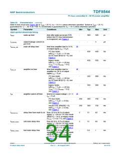
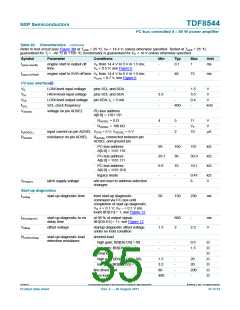
Table 20. Characteristics …continued
Refer to test circuit (see Figure 30) at Tamb = 25 C; VP = 14.4 V; unless otherwise specified. Tested at Tamb = 25 C;
guaranteed for Tj = 40 C to +150 C; functionality is guaranteed for VP < 10 V unless otherwise specified.
Symbol
Parameter
Conditions
Min
Typ
Max
Unit
t(start-Vo(off))
engine start to output off
time
VP from 14.4 V to 5 V in 1.5 ms;
Vo < 0.5 V; see Figure 6
-
0.1
1
ms
t(start-SVRoff)
engine start to SVR off time VP from 14.4 V to 5 V in 1.5 ms;
VSVR < 0.7 V; see Figure 6
-
40
-
75
ms
I2C-bus interface[3]
VIL
LOW-level input voltage
pins SCL and SDA
pins SCL and SDA
pin SDA; IL = 5 mA
-
1.5
5.5
0.4
-
V
VIH
HIGH-level input voltage
LOW-level output voltage
SCL clock frequency
2.3
V
VOL
-
-
-
V
fSCL
VADSEL
400
kHz
voltage on pin ADSEL
I2C-bus address
A[6:0] = 1101 101
RADSEL = 0
4
-
5
-
11
VP
10
V
RADSEL = 100 k
V
II(ADSEL)
RADSEL
input current on pin ADSEL VSTB = 5 V; VADSEL = 5 V
-
2
A
resistance on pin ADSEL
RADSEL connected between pin
ADSEL and ground pin
I2C-bus address
A[6:0] = 1101 110
I2C-bus address
A[6:0] = 1101 111
I2C-bus address
A[6:0] = 1101 010
99
29.7
9.9
-
100
30
10
-
101
k
k
k
30.3
10.1
legacy mode
0.47
6
k
VP(latch)
latch supply voltage
will not react to address selection
changes
V
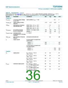
Start-up diagnostics
tsudiag
start-up diagnostic time
from start-up diagnostic
50
130
250
ms
command via I2C-bus until
completion of start-up diagnostic;
VO + < 0.1 V; VO < 0.1 V (no
load) IB1[D1] = 1; see Figure 12
td(sudiag-on)
Voffset
start-up diagnostic to on
delay time
at 90 % of output signal;
IB1[D0:D1] = 11; see Figure 12
-
680
2
-
ms
V
offset voltage
startup diagnostic offset voltage
under no load condition
1.3
2.5
RLdet(sudiag)
start-up diagnostic load
detection resistance
shorted load
high gain; IB3[D6:D5] = 00
low gain; IB3[D6:D5] = 11
normal load:
-
-
-
-
0.5
1.5
high gain (IB3[D6:D5] = 00)
low gain (IB3[D6:D5] = 11)
line driver load
1.5
3.2
80
-
-
-
-
20
20
200
-
open load
400
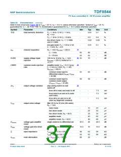
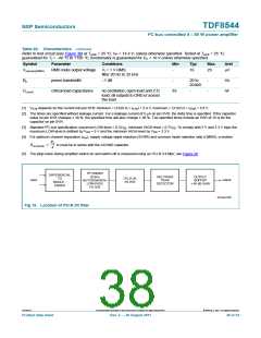
TDF8544
All information provided in this document is subject to legal disclaimers.
© NXP B.V. 2011. All rights reserved.
Product data sheet
Rev. 2 — 29 August 2011
35 of 54

 NXP [ NXP ]