TDF8544
NXP Semiconductors
I2C-bus controlled 4 50 W power amplifier
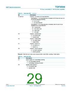
Table 17. Data byte DB5 …continued
Bit
Description
D3
VP below above 10 V
0 = VP above 10 V
1 = VP has dropped below 10 V
undervoltage protection
D2
0 = no undervoltage protection occurred
1 = undervoltage protection occurred (engine start)
-
amplifier and output stage status[1]
0 = amplifier switched off, output stage high impedance
1 = amplifier switched on, output stage active
D1
D0
[1] Bits DB5[D0] and [D5] are not latched/cleared after being read. They indicate the actual value.
Remark: Data bits are only reset (cleared after read) after reading all 5 data bytes.
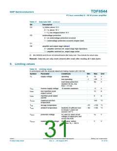
9. Limiting values
Table 18. Limiting values
In accordance with the Absolute Maximum Rating System (IEC 60134).
Symbol
Parameter
Conditions
operating
Min
6
Max
18
Unit
V
VP
supply voltage
non-operating
1
-
+50
50
V
load dump protection;
duration 50 ms, rise
time > 2.5 ms
V
VP(r)
IOSM
reverse supply voltage
10 minutes maximum
-
-
2
V
A
non-repetitive peak
output current
13
IORM
repetitive peak output
current
-
-
8
A
Tj(max)
maximum junction
temperature
150
C
Tstg
storage temperature
ambient temperature
55
40
+150
+105
C
C
Tamb
heatsink of sufficient size
to ensure Tj does not
exceed 150 C
V(prot)
protection voltage
AC and DC short-circuit
voltage of output pins and
across the load
-
-
VP
5
V
V
Vi(max)
maximum input voltage RMS value; before
capacitor; RS = 100
TDF8544
All information provided in this document is subject to legal disclaimers.
© NXP B.V. 2011. All rights reserved.
Product data sheet
Rev. 2 — 29 August 2011
31 of 54

 NXP [ NXP ]