TDF8544
NXP Semiconductors
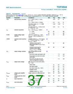
I2C-bus controlled 4 50 W power amplifier
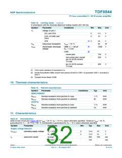
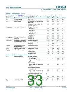
Table 20. Characteristics …continued
Refer to test circuit (see Figure 30) at Tamb = 25 C; VP = 14.4 V; unless otherwise specified. Tested at Tamb = 25 C;
guaranteed for Tj = 40 C to +150 C; functionality is guaranteed for VP < 10 V unless otherwise specified.
Symbol
Ioff
Parameter
Conditions
Min
-
Typ
4
Max
10
Unit
A
V
off-state current
output voltage
VSTB = 0.4 V
VO
DC; amplifier on; high gain/low
gain mode
6.6
7.1
7.6
line driver mode; IB4[D2] = 0;
IB3[D5] = [D6] = 1
3.0
3.4
3.8
V
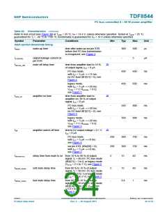
VP(low)(mute)
low supply voltage mute
rising supply voltage
IB4[D0] = 1
7.0
5.4
7.7
5.7
8.1
6.2
V
V
IB4[D0] = 0
falling supply voltage
IB4[D0] = 1
6.5
5.2
0.1
0.1
15.2
14.4
-
7.2
5.5
0.5
0.3
16
7.7
5.9
0.8
0.7
16.9
16.2
-
V
V
V
V
V
V
V
V
IB4[D0] = 0
VP(low)(mute)
low supply voltage mute
hysteresis
IB4[D0] = 1
IB4[D0] = 0
VP(ovp)pwarn
pre-warning overvoltage
protection supply voltage
rising supply voltage
falling supply voltage
hysteresis
15.2
0.8
20
Vth(ovp)
overvoltage protection
threshold voltage
rising supply voltage
18
22
VPOR
power-on reset voltage
output offset voltage
falling supply voltage
amplifier on
-
3.1
0
4.5
V
VO(offset)
75
25
45
+75
+25
+45
mV
mV
mV
amplifier mute
0
line driver mode
0
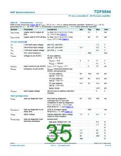
Mode select and second clip detection: pin STB
VSTB
voltage on pin STB
off mode selected
I2C-bus mode
-
-
-
-
0.8
0.8
V
V
legacy mode (I2C-bus mode
off)
mute selected
legacy mode (I2C-bus mode
off)
2.5
-
4.5
V
operating mode selected
I2C-bus mode
legacy mode (I2C-bus mode
off)
2.5
5.9
-
-
VP
VP
V
V
[1]
[1]
low voltage on pin STB when
pulled LOW during clipping
ISTB = 150 A
ISTB = 500 A
5.6
6.1
-
5.9
-
6.5
7.4
30
V
V
ISTB
current on pin STB
0 V < VSTB < 8.5 V; clip detection
not active
5
A
TDF8544
All information provided in this document is subject to legal disclaimers.
© NXP B.V. 2011. All rights reserved.
Product data sheet
Rev. 2 — 29 August 2011
33 of 54

 NXP [ NXP ]