TDF8544
NXP Semiconductors
I2C-bus controlled 4 50 W power amplifier
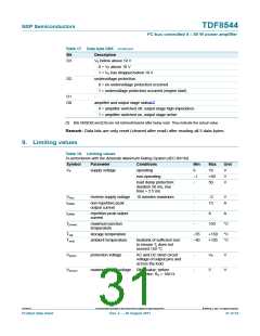
Table 18. Limiting values …continued
In accordance with the Absolute Maximum Rating System (IEC 60134).
Symbol
Parameter
Conditions
Min
Max
Unit
Vx
voltage on pin x
SCL and SDA
0
0
6.5
10
V
V
SVR, ACGND and
DIAG
[1]
STB
0
-
24
V
Ptot
total power dissipation
Tcase = 70 C
80
W
V
[2]
[3]
VESD
electrostatic discharge
voltage
HBM; C = 100 pF;
Rs = 1.5 k
-
2000
CDM
corner pins
-
-
750
500
V
V
non-corner pins; except
pin 24 (SVR) version
TH only
pin 24 (SVR) version
TH only
-
400
V
[1] 10 k series resistance if connected to VP.
[2] Human Body Model (HBM): all pins have passed all tests to 2500 V to guarantee 2000 V, according to
class II.
[3] Charged-Device Model (CDM).
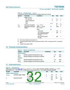
10. Thermal characteristics
Table 19. Thermal characteristics
Symbol Parameter
DBS27/RDBS27
Conditions
Typ
Unit
Rth(j-c)
thermal resistance from junction to case
1.15
40
K/W
K/W
Rth(j-a)
HSOP36
Rth(j-c)
thermal resistance from junction to ambient
thermal resistance from junction to case
thermal resistance from junction to ambient
1.15
35
K/W
K/W
Rth(j-a)
11. Characteristics
Table 20. Characteristics
Refer to test circuit (see Figure 30) at Tamb = 25 C; VP = 14.4 V; unless otherwise specified. Tested at Tamb = 25 C;
guaranteed for Tj = 40 C to +150 C; functionality is guaranteed for VP < 10 V unless otherwise specified.
Symbol
Supply voltage behavior
VP(oper) operating supply voltage
Parameter
Conditions
Min
Typ
Max
Unit
RL = 4
6
6
-
14.4
14.4
260
190
18
16
350
-
V
RL = 2
V
Iq
quiescent current
no load
mA
mA
no load; VP = 7 V
-
TDF8544
All information provided in this document is subject to legal disclaimers.
© NXP B.V. 2011. All rights reserved.
Product data sheet
Rev. 2 — 29 August 2011
32 of 54

 NXP [ NXP ]