TDF8544
NXP Semiconductors
I2C-bus controlled 4 50 W power amplifier
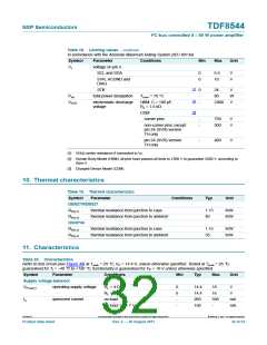
Table 20. Characteristics …continued
Refer to test circuit (see Figure 30) at Tamb = 25 C; VP = 14.4 V; unless otherwise specified. Tested at Tamb = 25 C;
guaranteed for Tj = 40 C to +150 C; functionality is guaranteed for VP < 10 V unless otherwise specified.
Symbol
Parameter
Conditions
Min
Typ
Max
Unit
Diagnostic
VOL(DIAG)
LOW-level output voltage
on pin DIAG
fault condition; IDIAG = 1 mA
-
-
0.3
V
V
VO(offset_det)
THDclip
output voltage at offset
detection
1.0
1.3
2.0
total harmonic distortion
clip detection level
IB2[D7:D6] = 10; VP > 10 V
IB2[D7:D6] = 01; VP > 10 V
IB2[D7:D6] = 00; VP > 10 V
IB3[D4] = 0 or legacy mode
IB3[D4] = 1
-
10
5
-
%
-
-
%
-
2
-
%
Tj(AV)(pwarn)
pre-warning average
junction temperature
150
125
-
160
135
175
170
145
-
C
C
C
Tj(AV)(G(0.5dB)) average junction
temperature for 0.5 dB gain
Vi = 0.05 V
reduction
G(th_fold)
gain reduction of thermal
foldback
all channels will switch off
-
20
-
dB
Io
output current
I2C-bus mode; AC load bit set;
peak current
IB4[D1] = 1
580
320
-
-
-
-
mA
mA
IB4[D1] = 0
I2C-bus mode; AC load bit not
set; peak current
IB4[D1] = 1
IB4[D1] = 0
-
-
-
-
250
125
mA
mA
Amplifier
Po
output power
RL = 4 ; VP = 14.4 V;
THD = 0.5 %
19
26
34
45
40
47
70
22
28
37
51
44
50
75
-
-
-
-
-
-
-
W
W
W
W
W
W
W
RL = 4 ; VP = 14.4 V;
THD = 10 %
RL = 2 ; VP = 14.4 V;
THD = 0.5 %
RL = 2 ; VP = 14.4 V;
THD = 10 %
maximum output power
RL = 4 ; VP = 14.4 V;
Vi = 2 V RMS square wave
Po(max)
RL = 4 ; VP = 15.2 V;
Vi = 2 V RMS square wave
RL = 2 ; VP = 14.4 V;
Vi = 2 V RMS square wave
TDF8544
All information provided in this document is subject to legal disclaimers.
© NXP B.V. 2011. All rights reserved.
Product data sheet
Rev. 2 — 29 August 2011
36 of 54

 NXP [ NXP ]