TDF8544
NXP Semiconductors
I2C-bus controlled 4 50 W power amplifier
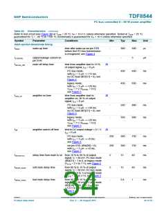
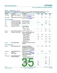
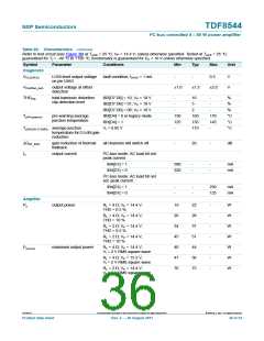
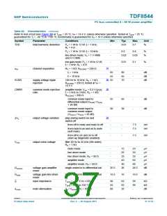
Table 20. Characteristics …continued
Refer to test circuit (see Figure 30) at Tamb = 25 C; VP = 14.4 V; unless otherwise specified. Tested at Tamb = 25 C;
guaranteed for Tj = 40 C to +150 C; functionality is guaranteed for VP < 10 V unless otherwise specified.
Symbol
Parameter
Conditions
Min
Typ
Max
Unit
Vo(mute)(RMS)
RMS mute output voltage
Vi = 1 V RMS;
-
16
29
V
filter 20 Hz to 22 kHz
Bp
power bandwidth
1 dB
-
20 to
20000
-
-
Hz
nF
CL(crit)
critical load capacitance
no oscillation; open load and 2
load; all outputs to GND or across
the load
33
-
[1] VSTB depends on the current into pin STB: minimum = (1429 ISTB) + 5.4 V, maximum = (3143 ISTB) + 5.6 V.
[2] The times are specified without leakage current. For a leakage current of 5 A on pin SVR, the delta time is specified. If the capacitor
value on pin SVR changes 30 %, the specified time will also change 30 %. The specified times include an ESR of 15 for the
capacitor on pin SVR.
[3] Standard I2C-bus specification: maximum LOW-level = 0.3VDD, minimum HIGH-level = 0.7VDD. To comply with 5 V and 3.3 V logic the
maximum LOW-level is defined by VDD = 5 V and the minimum HIGH-level by VDD = 3.3 V.
[4] For optimum channel separation (cs), supply voltage ripple rejection (SVRR) and common mode rejection ratio (CMRR), a resistor
RS
-----
RACGND
=
must be in series with the ACGND capacitor.
4
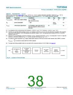
[5] The plop-noise during amplifier switch-on and switch-off is measured using an ITU-R 2 k filter; see Figure 20.
th
5
ORDER
20 kHz
DIFFERENTIAL
TO
SINGLE −
ENDED
RECTIFIER
PEAK
DETECTOR
OUTPUT
BUFFER
+ 40 dB GAIN
ITU-R 2K
FILTER
input
output
BUTTERWORTH
LOW-PASS
FILTER
001aam706
Fig 19. Location of ITU-R 2K filter
TDF8544
All information provided in this document is subject to legal disclaimers.
© NXP B.V. 2011. All rights reserved.
Product data sheet
Rev. 2 — 29 August 2011
38 of 54

 NXP [ NXP ]