TDF8544
NXP Semiconductors
I2C-bus controlled 4 50 W power amplifier
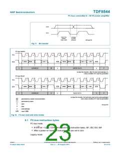
SDA
SCL
data line
stable;
data valid
change
of data
allowed
001aam704
Fig 17. Bit transfer
2
I C-bus WRITE
SCL
SDA
1
2
7
8
9
1
2
7
8
9
MSB
MSB − 1
LSB + 1
LSB
MSB
MSB − 1
LSB + 1
ACK
ACK
S
ADDRESS
A
WRITE DATA
A
P
W
to stop the transfer, after the last acknowledge (A)
a stop condition (P) must be generated
2
I C-bus READ
SCL
SDA
1
2
7
8
9
1
2
7
8
9
MSB
MSB − 1
LSB + 1
MSB
MSB − 1
LSB + 1
LSB
ACK
A
ACK
S
R
A
P
ADDRESS
READ DATA
to stop the transfer, the last byte must not be acknowledged
and a stop condition (P) must be generated
: generated by master (microcontroller)
: generated by slave
: start
S
P
001aam705
: stop
A
: acknowledge
: read / write
R/W
Fig 18. I2C-bus read and write modes
8.1 I2C-bus instruction bytes
I2C-bus mode:
• If R/W bit = 0, the TDF8544 expects four instruction bytes; IB1, IB2, IB3, IB4
• After a power-on reset, all instruction bits are set to zero
Legacy mode:
TDF8544
All information provided in this document is subject to legal disclaimers.
© NXP B.V. 2011. All rights reserved.
Product data sheet
Rev. 2 — 29 August 2011
23 of 54

 NXP [ NXP ]