TDF8544
NXP Semiconductors
I2C-bus controlled 4 50 W power amplifier
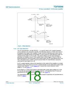
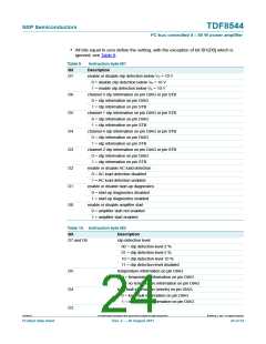
Cleared after read means that the I2C-bus bits are cleared after a read command. The
Clear command is done only if all five data bytes are read. If only four data bytes are read,
the I2C-bus latches are not cleared and the old value remains in the latches.
When selected, pin DIAG gives actual diagnostic information. If a failure is removed,
pin DIAG is released instantly, independently of the I2C-bus latches.
7.8 Amplifier in combination with a DC-to-DC converter
The TDF8544 can be used in combination with a DC-DC up-converter as the supply for
the amplifier (connected to VP). If the DC-DC converter output voltage is controlled with
the audio signal, the amplifier’s dissipation can be reduced at lower output powers. To
ensure that the amplifier can follow supply voltage variations, the supply voltage ripple
capacitor connected to pin SVR, to filter the amplifier’s common mode output voltage,
must be disconnected internally. The SVR capacitor is still used to determine the DC input
voltage. If I2C-bus bit IB4[D7] = 1, the common mode output voltage directly follows the
supply voltage variations.
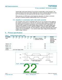
8. I2C-bus specification
Table 8.
Pin ADSEL
Open
TDF8544 hardware address select
A6
A5
A4
A3
A2
A1
A0
R/W
Hex
Remark
1
1
0
1
1
0
0
0 = write to TDF8544;
1 = read from TDF8544
D8
reserved;
instruction and
data bytes
have other
meaning
100 k 1 %
30 k 1 %
10 k 1 %
Voltage > 4 V
Ground
1
1
1
0
0
1
0
1
DC
DE
D4
DA
-
-
-
-
-
0
1
no I2C-bus; legacy mode
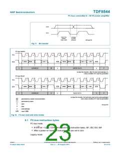
SDA
SCL
S
P
SDA changes when SCL is HIGH:
STOP condition
001aam703
START condition
start − or stop condition
Fig 16. Definition of START and STOP conditions
TDF8544
All information provided in this document is subject to legal disclaimers.
© NXP B.V. 2011. All rights reserved.
Product data sheet
Rev. 2 — 29 August 2011
22 of 54

 NXP [ NXP ]