TDF8544
NXP Semiconductors
I2C-bus controlled 4 50 W power amplifier
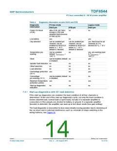
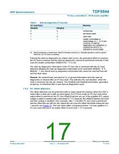
Table 5.
Start-up diagnostics I2C-bus bits
DC load bits[1]
Meaning
DBx[D5]
DBx[D4]
0
0
1
1
0
1
0
1
normal load
line driver mode
open load
invalid: overvoltage or
undervoltage (VP < 10 V) has
occurred, or start-up
diagnostics not completed, or
channel has short to VP;
indicated in second stage
[1] DBx[D3] indicates a shorted load; DBx[D1] indicates a short to VP; DBx[D0] indicates a short to ground.
When set, D4, D5 have no meaning.
If during the start-up diagnostics an engine start occurs, the generated offset to measure
the DC load is reduced and the start-up diagnostics cannot be performed correctly. In this
case the invalid combination DBx[D4:D5] = 11 is set.
The start-up diagnostics information in the I2C-bus bits is combined with the AC load
detection allowing the start-up diagnostics information to be read when IB4[D4] = 0. If
IB4[D4] = 1, the stored start-up diagnostics information bits cannot be read but they will
not lose their value.
Remark: the shorted load, and short to VP or ground information from the start-up
diagnostics is cleared after an I2C-bus read. This indicates the real situation: when the
short is removed, the bits are cleared. The DBx[D5] and DBx[D4] information, generated
at start-up, is refreshed after a new start-up diagnostics cycle.
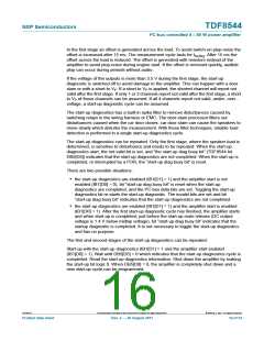
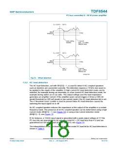
7.5.2 DC offset detection
The offset detection can be performed with no input signal (for instance when the DSP is
muted after a start-up) or with an input signal. If in I2C-bus mode an I2C-bus read of the
output offset is performed, the I2C-bus DBx[D2] latches are set. If the amplifier BTL output
voltage is within a window with a threshold of 1.3 V (typical), the DBx[D2] latches are reset
and their setting is disabled. If for example, after 1 s another I2C-bus read is performed
and the offset bits are still set, the output did not cross the offset threshold during the last
1 second; see Figure 13. This can mean either a frequency below 1 Hz was applied (1 s
I2C-bus read interval) or an output offset of more than 1.3 V is present.
TDF8544
All information provided in this document is subject to legal disclaimers.
© NXP B.V. 2011. All rights reserved.
Product data sheet
Rev. 2 — 29 August 2011
17 of 54

 NXP [ NXP ]