®
Numonyx™ StrataFlash Embedded Memory (J3-65nm)
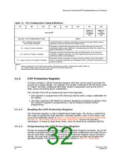
Table 12: STS Configuration Coding Definitions
D7
D6
D5
D4
D3
D2
D1
D0
Pulse on
Program
Complete
(1)
Pulse on
Erase
Complete
(1)
3
Reserved
D[1:0] = STS Configuration Codes
Notes
00 = default, level mode;
device ready indication
Controls HOLD to a memory controller to prevent accessing a flash memory
subsystem while any flash device's WSM is busy.
Generates a system interrupt pulse when any flash device in an array has
completed a block erase. Helpful for reformatting blocks after file system free
space reclamation or “cleanup.”
01 = pulse on Erase Complete
10 = pulse on Program Complete
Generate a system interrupt pulse when any flash device in an array has
complete a Program operation. Provides highest performance for servicing
continuous buffer write operations.
Generates system interrupts to trigger servicing of flash arrays when either
erase or program operations are completed, when a common interrupt service
routine is desired.
11 = pulse on Erase or Program Complete
Notes:
1.
2.
3.
When configured in one of the pulse modes, STS pulses low with a typical pulse width of 500 ns.
An invalid configuration code will result in both SR.4 and SR.5 being set.
Reserved bits are invalid should be ignored.
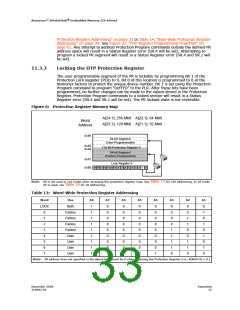
11.3
OTP Protection Register
J3-65nm includes a 128-bit Protection Register (PR) that can be used to increase the
security of a system design. For example, the number contained in the PR can be used
to “match” the flash component with other system components such as the CPU or
ASIC, hence preventing device substitution.
The 128-bits of the PR are divided into two 64-bit segments:
• One segment is programmed at the Numonyx factory with a unique unalterable 64-
bit number.
• The other segment is left blank for customer designers to program as desired. Once
the customer segment is programmed, it can be locked to prevent further
programming.
11.3.1
11.3.2
Reading the OTP Protection Register
The Protection Register is read in Identification Read mode. The device is switched to
this mode by issuing the Read Identifier command (0090h). Once in this mode, read
cycles from addresses shown in Table 13, “Word-Wide Protection Register Addressing”
or Table 14, “Byte-Wide Protection Register Addressing” retrieve the specified
information. To return to Read Array mode, write the Read Array command (00FFh).
Programming the OTP Protection Register
PR bits are programmed using the two-cycle Protection Program command. The 64-bit
number is programmed 16 bits at a time for word-wide configuration and eight bits at a
time for byte-wide configuration. First write the Protection Program Setup command,
00C0h. The next write to the device will latch in address and data and program the
specified location. The allowable addresses are shown in Table 13, “Word-Wide
Datasheet
32
December 2008
319942-02

 NUMONYX [ NUMONYX B.V ]