®
Numonyx™ StrataFlash Embedded Memory (J3-65nm)
12.0
Power and Reset Specifications
12.1
Power-Up and Power-Down
Power supply sequencing is not required if VPEN is connected to VCC or VCCQ.
Otherwise VCC and VCCQ should attain their minimum operating voltage before
applying VPEN.
Power supply transitions should only occur when RP# is low. This protects the device
from accidental programming or erasure during power transitions.
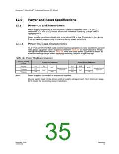
12.1.1
Power-Up/Down Characteristics
To prevent conditions that could result in spurious program or erase operations, several
valid power-up/power-down sequences shown in Table 15 are recommended. For DC
voltage characteristics refer to Table 20. Note that each power supply must reach its
minimum voltage range before applying/removing the next supply voltage.
Table 15: Power-Up/Down Sequence
Power Supply
Power-Up Sequence
Power-Down Sequence
Voltage
V
1st
2nd
3rd
1st
3rd
2nd
1st
2nd
CC(min)
†
†
1st
2nd
Sequencingnot
Sequencingnot
V
†
†
CCQ(min)
required
required
†
†
2nd
1st
V
2nd
1st
PEN(min)
Note:
Power supplies connected or sequenced together.
Device inputs must not be driven until all supply voltages reach their minimum range.
RP# should be low during power transitions.
December 2008
319942-02
Datasheet
35

 NUMONYX [ NUMONYX B.V ]