®
Numonyx™ StrataFlash Embedded Memory (J3-65nm)
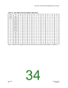
Protection Register Addressing” on page 33 or Table 14, “Byte-Wide Protection Register
Addressing” on page 34. See Figure 22, “OTP Register Programming Flowchart” on
page 62. Any attempt to address Protection Program commands outside the defined PR
address space will result in a Status Register error (SR.4 will be set). Attempting to
program a locked PR segment will result in a Status Register error (SR.4 and SR.1 will
be set).
11.3.3
Locking the OTP Protection Register
The user-programmable segment of the PR is lockable by programming Bit 1 of the
Protection Lock Register (PLR) to 0. Bit 0 of this location is programmed to 0 at the
Numonyx factory to protect the unique device number. Bit 1 is set using the Protection
Program command to program “0xFFFD” to the PLR. After these bits have been
programmed, no further changes can be made to the values stored in the Protection
Register. Protection Program commands to a locked section will result in a Status
Register error (SR.4 and SR.1 will be set). The PR lockout state is not reversible.
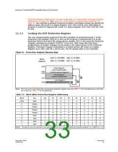
Figure 6: Protection Register Memory Map
A[24:1]: 256 Mbit A[22:1]: 64 Mbit
A[23:1]: 128 Mbit A[21:1]: 32 Mbit
Word
Address
0x88
64-bit Segment
(User-Programmable)
0x85
0x84
128-Bit Protection Register 0
64-bit Segment
(Factory-Programmed)
0x81
0x80
Lock Register 0
15 14 13 12 11 10
9
8
7
6
5
4
3
2
1
0
Note: A0 is not used in x16 mode when accessing the protection register map. See Table 13 for x16 addressing. In x8 mode
A0 is used, see Table 14 for x8 addressing.
Table 13: Word-Wide Protection Register Addressing
Word
Use
A8
A7
A6
A5
A4
A3
A2
A1
LOCK
Both
Factory
Factory
Factory
Factory
User
1
1
1
1
1
1
1
1
1
0
0
0
0
0
0
0
0
0
0
0
0
0
0
0
0
0
0
0
0
0
0
0
0
0
0
0
0
0
0
0
0
0
0
0
1
0
0
0
0
1
1
1
1
0
0
0
1
1
0
0
1
1
0
0
1
0
1
0
1
0
1
0
0
1
2
3
4
5
6
7
User
User
User
Note: All address lines not specified in the above table must be 0 when accessing the Protection Register (i.e., A[MAX:9] = 0.)
December 2008
319942-02
Datasheet
33

 NUMONYX [ NUMONYX B.V ]