®
Numonyx™ StrataFlash Embedded Memory (J3-65nm)
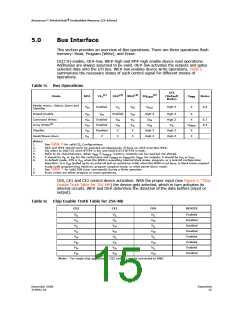
5.0
Bus Interface
This section provides an overview of Bus operations. There are three operations flash
memory: Read, Program (Write), and Erase.
CE[2:0]-enable, OE#-low, WE#-high and RP#-high enable device read operations.
Addresses are always assumed to be valid. OE#-low activates the outputs and gates
selected data onto the I/O bus. WE#-low enables device write operations. Table 5
summarizes the necessary states of each control signal for different modes of
operations.
Table 5:
Bus Operations
STS
(Default
Mode)
(1)
(2)
(2)
(3)
15:0
Mode
RP#
CE
OE#
WE#
DQ
V
Notes
x
PEN
Reads: Async., Status, Query and
Identifier
V
Enabled
V
V
V
D
OUT
High-Z
X
4,6
IH
IL
IH
Output Disable
V
V
V
V
V
Enabled
High-Z
High-Z
High Z
X
X
IH
IH
IH
IH
IH
IH
Command Writes
Enabled
Enabled
Disabled
X
V
V
V
V
D
D
6,7
8,5
IH
IH
IL
IL
IN
IN
(8)
Array Writes
V
V
IL
PENH
Standby
X
X
High Z
High Z
High Z
High Z
X
Reset/Power-down
Notes:
V
X
X
X
IL
1.
2.
3.
4.
5.
6.
See Table 6 for valid CE Configurations.
x
OE# and WE# should never be asserted simultaneously. If done so, OE# overrides WE#.
DQ refers to DQ[7:0] when BYTE# is low and DQ[15:0] if BYTE# is high.
Refer to DC characteristics. When VPEN ≤ V
, memory contents can be read but not altered.
PENLK
X should be V or V for the control pins and V
or V
for V
. For outputs, X should be V or V
.
OH
IL
IH
PENLK
PENH
PEN
OL
In default mode, STS is V when the WSM is executing internal block erase, program, or a lock-bit configuration
OL
algorithm. It is V (pulled up by an external pull up resistance ≈10k) when the WSM is not busy, in block erase suspend
OH
mode (with programming inactive), program suspend mode, or reset power-down mode.
See Table 7 for valid DIN (user commands) during a Write operation
Array writes are either program or erase operations.
7.
8.
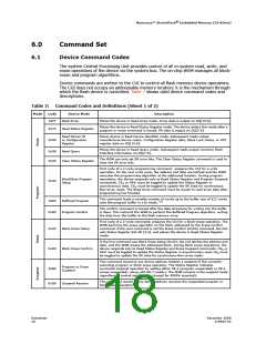
CE0, CE1 and CE2 control device activation. With the proper input (see Figure 6, “Chip
Enable Truth Table for 256-Mb) the device gets selected, which in turn activates its
internal circuits. WE# and OE# determine the direction of the data buffers (input or
output).
Table 6:
Chip Enable Truth Table for 256-Mb
CE2
CE1
CE0
DEVICE
V
V
V
V
V
V
V
Enabled
Disabled
Disabled
Disabled
Enabled
Enabled
Enabled
Disabled
IL
IL
IL
IL
IL
V
IH
V
V
V
IL
IH
IH
IL
V
IL
IH
V
V
V
V
V
V
V
IH
IH
IH
IH
IL
IL
IL
V
IH
V
V
V
IH
IH
IL
V
IH
Note: For single-chip applications, CE2 and CE1 can be connected to GND.
December 2008
319942-02
Datasheet
15

 NUMONYX [ NUMONYX B.V ]