®
Numonyx™ StrataFlash Embedded Memory (J3-65nm)
6.0
Command Set
6.1
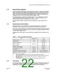
Device Command Codes
The system Central Processing Unit provides control of all in-system read, write, and
erase operations of the device via the system bus. The on-chip WSM manages all block-
erase and program algorithms.
Device commands are written to the CUI to control all flash memory device operations.
The CUI does not occupy an addressable memory location; it is the mechanism through
which the flash device is controlled. Table 7 shows valid device command codes and
descriptions.
Table 7:
Command Codes and Definitions (Sheet 1 of 2)
Mode
Code
Device Mode
Read Array
Description
0xFF
0x70
Places the device in Read Array mode. Array data is output on DQ[15:0].
Places the device in Read Status Register mode. The device enters this mode after a
program or erase command is issued. SR data is output on DQ[7:0].
Read Status Register
Read Device ID
or Configuration
Register
Places device in Read Device Identifier mode. Subsequent reads output
manufacturer/device codes, Configuration Register data, Block Lock status, or OTP
register data on DQ[15:0].
0x90
Places the device in Read Query mode. Subsequent reads output Common Flash
Interface information on DQ[7:0].
0x98
0x50
Read Query
The WSM can only set SR error bits. The Clear Status Register command is used to
clear the SR error bits.
Clear Status Register
First cycle of a 2-cycle programming command, prepares the CUI for a write
operation. On the next write cycle, the address and data are latched and the WSM
executes the programming algorithm at the addressed location. During program
operations, the device responds only to Read Status Register and Program Suspend
Word/Byte Program
Setup
0x40
commands. CE or OE# must be toggled to update the Status Register in
X
asynchronous read. CE must be toggled to update the SR Data for synchronous
X
Non-array reads. The Read Array command must be issued to read array data after
programming has finished.
This command loads a variable number of words up to the buffer size of 512 words
0xE8
0xD0
Buffered Program
Program Confirm
(1)
onto the program buffer in x16 mode.
The confirm command is Issued after the data streaming for writing into the buffer
is done. This instructs the WSM to perform the Buffered Program algorithm, writing
the data from the buffer to the flash memory array.
First cycle of a 2-cycle command; prepares the CUI for a block-erase operation. The
WSM performs the erase algorithm on the block addressed by the Erase Confirm
command. If the next command is not the Erase Confirm (0xD0) command, the CUI
sets Status Register bits SR [5,4], and places the device in Read Status Register
mode.
0x20
0xD0
Block Erase Setup
If the first command was Block Erase Setup (0x20), the CUI latches the address and
data, and the WSM erases the addressed block. During block-erase operations, the
Block Erase Confirm
device responds only to Read Status Register and Erase Suspend commands. CE or
X
OE# must be toggled to update the Status Register in asynchronous read. CE must
X
be toggled to update the SR Data for synchronous Non-array reads.
This command issued to any device address initiates a suspend of the currently-
executing program or block erase operation. The Status Register indicates
successful suspend operation by setting either SR.2 (program suspended) or SR 6
(erase suspended), along with SR.7 (ready). The WSM remains in the suspend mode
regardless of control signal states (except for RPRP# asserted).
Program or Erase
Suspend
0xB0
0xD0
This command issued to any device address resumes the suspended program or
block-erase operation.
Suspend Resume
Datasheet
18
December 2008
319942-02

 NUMONYX [ NUMONYX B.V ]